DFM design sharing of PCB inner layer
PCB engineers layout a product, not only layout and wiring, but also the design of inner power plane and ground plane is very important. In dealing with the inner layer, we must not only consider power integrity, signal integrity, electromagnetic compatibility, but also DFM manufacturability.
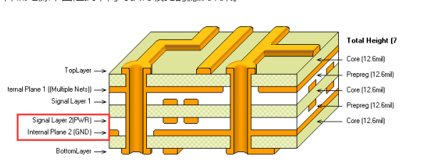
The difference between the inner layer and the surface layer of the PCB is that the surface layer is used to route and solder components, while the inner layer is used to plan the power/ground layer. This layer is only used for multi-layer boards and is mainly used to arrange power lines and ground lines. We call them double-layer boards, four-layer boards, and six-layer boards, which usually refer to the number of signal layers and internal power/ground layers.
Inner layer design
Design the ground layer below key signals such as high-speed signals, test signals, and high-frequency signals, so that the path of the signal loop is the shortest and the radiation is the smallest.
In the process of high-speed circuit design, it is necessary to consider how to deal with the radiation of the power supply and the interference to the entire system. Generally, the area of the power layer plane should be smaller than the area of the ground plane, so that the power supply can be shielded. Generally, the power plane is required to be indented by 2 times the dielectric thickness of the ground plane.
Layer planning
The power plane is adjacent to the corresponding ground plane. The purpose is to form a coupling capacitor and work together with the decoupling capacitor on the PCB board to reduce the impedance of the power plane and obtain a wider filtering effect.
Reference plane
The selection of the reference layer is very important. In theory, both the power layer and the ground plane can be used as reference layers, but the ground plane can generally be grounded, and the shielding effect is much better than the power layer, so the ground plane is generally preferred as the reference plane.
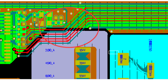
Signal lines cannot be routed across regions
The key signals of two adjacent layers cannot cross the partition area, otherwise a larger signal loop will be formed, resulting in stronger radiation and coupling.
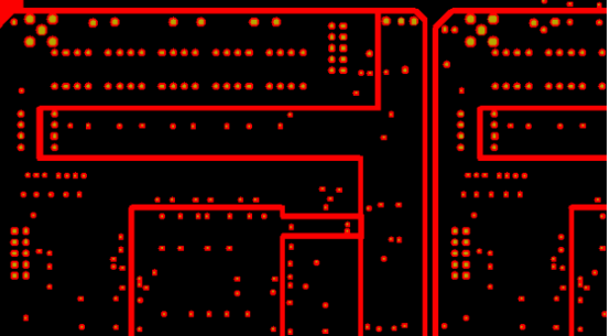
Power and ground routing planning
To maintain the integrity of the ground plane, routing cannot be done on the ground plane. If the signal line density is too large, routing can be considered on the edge of the power layer.
Inner layer manufacturing
Due to the complex process flow of PCB manufacturing, the process of inner layer manufacturing is only a part of it. When producing inner layer boards, it is also necessary to consider the process of other processes that affect the manufacturing capacity of the inner layer. For example, the press tolerance and drilling tolerance will affect the quality yield of the inner layer.
PCBs can be divided into single-sided boards, double-sided boards, and multi-layer boards according to the number of layers. The process flow of these three boards is also very different. Especially for multi-layer boards, the production process is much more complicated than that of single-sided and double-sided boards. Therefore, when designing multi-layer boards, it is necessary to consider the complex process flow and DFM manufacturability design of multi-layer boards.
Delete independent pads
Independent pads are non-functional PADs that are not connected to any network in the inner layer. Independent pads will be cancelled during the PCB manufacturing process. Because the cancellation of this independent pad has no effect on the design function of the product, it will affect the quality and production efficiency during manufacturing.

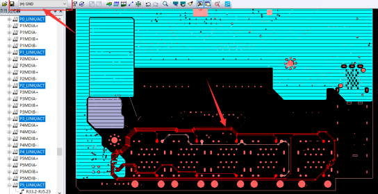
Inner layer BGA area
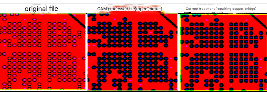
BGA devices are relatively small and have many pins, so the fan-out vias are very dense. During the manufacturing process, a certain distance needs to be maintained from drilling to routing and copper foil, otherwise short circuits may occur during the press and drilling process. When ensuring that a certain distance is left between the drilling holes and the copper foil and routing, the copper between the holes cannot be retained, which will cause the network to open. Therefore, when CAM engineers process the BGA area, they need to pay attention to the copper open circuit between the holes and the copper bridge to ensure that the network connection is not disconnected after production.
Abnormal inner layer design
All the holes in the inner layer negative film have hole rings. When converted into positive film graphics, all holes are disconnected from the copper foil and completely isolated. Complete isolation means that the inner layer has no function and can be done without the inner layer. When manufacturing encounters this problem, they will confirm with the design engineer whether the design is abnormal and the inner layer copper foil has no network added, resulting in complete isolation.
Negative inner layer bottleneck
When designing the power layer and ground layer division in the inner layer, the bottleneck of network conduction will appear due to the dense vias. The copper bridge width of the power network conduction is not enough, which will cause the matching current to not pass, resulting in board burning. Some bottleneck positions are even directly open, resulting in product design failure.