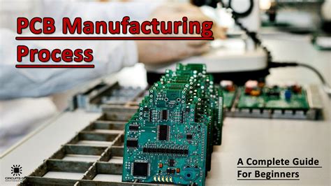
Essential Steps in PCB Assembly for Optimal Circuit Performance

Key Takeaways
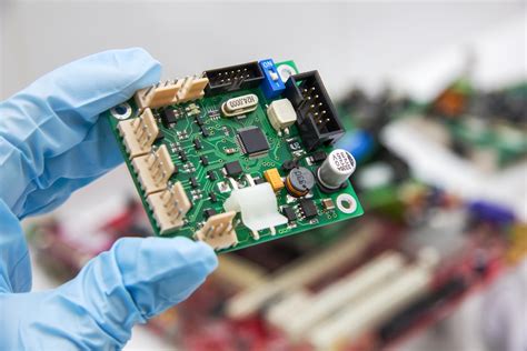
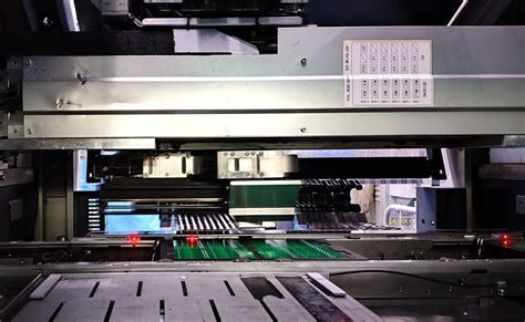
Successful PCB assembly (PCBA) hinges on meticulous attention to detail across every stage, from design verification to post-assembly quality assurance. The process begins with validating the board’s design against schematic requirements, ensuring compatibility with components and thermal profiles. Precision in component placement is critical, as misaligned parts can lead to signal interference or mechanical instability. Automated pick-and-place systems are often employed to achieve micron-level accuracy, especially for high-density boards.
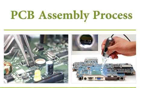
Advanced soldering methods, such as reflow or wave soldering, form reliable electrical connections while minimizing thermal stress. For surface-mount devices (SMDs), reflow soldering ensures uniform heat distribution, whereas through-hole components may require selective wave techniques. Post-soldering, automated optical inspection (AOI) and X-ray testing identify defects like solder bridges or voids, enabling timely corrections.
Tip: Early defect detection during inspection reduces rework costs and prevents performance issues in later stages.
Incorporating thermal management strategies—such as heat sinks or thermal vias—mitigates overheating risks, particularly in power-dense applications. Environmental factors, including humidity and chemical exposure, are addressed through protective coatings like conformal film, which shields circuits from corrosion. Finally, compliance checks validate adherence to industry standards (e.g., IPC-A-610), ensuring reliability under operational stress. By integrating these steps, PCBA delivers robust circuit performance while meeting functional and durability expectations.
Design Verification and Material Preparation
A successful PCB assembly process begins with rigorous design verification and meticulous material preparation. Before transitioning to production, engineers validate the PCBA design against schematics to ensure compatibility with functional requirements. This involves design rule checks (DRC) to confirm trace spacing, component clearances, and thermal management parameters. Simulation tools may also be employed to identify potential signal integrity issues or power distribution inefficiencies.
Material selection plays a pivotal role in achieving reliable PCB assembly outcomes. Key considerations include:
| Material Type | Role in PCBA | Common Options |
|---|---|---|
| Substrate | Base layer for circuitry | FR-4, Rogers, Polyimide |
| Solder Paste | Electrical/mechanical bonding | SAC305, Sn63/Pb37 |
| Components | Functional elements | SMDs, through-hole, BGAs |
| Conformal Coating | Environmental protection | Acrylic, Silicone, Urethane |
Component sourcing must prioritize authenticity and compatibility, as counterfeit or mismatched parts can lead to catastrophic failures. For PCBA, materials like high-temperature laminates or low-loss dielectrics are chosen based on application-specific demands, such as aerospace or consumer electronics.
Pre-production steps also involve generating Gerber files and assembly drawings to guide automated pick-and-place machinery. Stencils for solder paste application are tailored to the board’s layout, ensuring precise deposition. By addressing these foundational aspects, manufacturers minimize defects and lay the groundwork for optimal PCB assembly performance in subsequent stages.
Accurate Component Placement Techniques
Precise component placement is a cornerstone of effective PCB assembly, directly influencing the functionality and longevity of the final product. During the PCBA process, automated pick-and-place machines are utilized to position surface-mount devices (SMDs) and through-hole components with micrometer-level accuracy. These machines rely on computer-aided design (CAD) data to ensure alignment with the board’s layout, minimizing errors such as misalignment or tombstoning. For high-density interconnect (HDI) boards, where components are tightly packed, advanced vision systems and fiducial markers further enhance placement precision.
Critical to this stage is the correct orientation of polarized components, such as diodes or electrolytic capacitors, which must align with the circuit’s schematic to prevent malfunctions. Additionally, thermal management components like heat sinks or thermal pads require strategic placement to avoid hotspots and ensure efficient heat dissipation. Modern PCB assembly workflows often integrate real-time inspection systems, such as automated optical inspection (AOI), to verify placement accuracy before proceeding to soldering.
The choice of solder paste and stencil design also plays a role in component placement. A well-printed solder paste layer ensures proper adhesion during reflow soldering, reducing the risk of shifts or voids. For mixed-technology boards combining SMDs and through-hole parts, selective soldering or manual insertion may complement automated processes. By prioritizing meticulous component placement techniques, manufacturers can mitigate assembly defects, optimize electrical performance, and meet the rigorous demands of modern electronics.
Advanced Soldering Methods for Reliable Connections
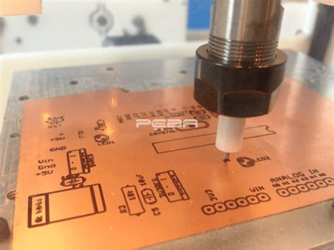
Achieving durable electrical connections in PCB assembly hinges on the application of advanced soldering techniques tailored to modern circuit complexity. Reflow soldering remains a cornerstone of PCBA, particularly for surface-mount devices (SMDs), where precise temperature profiles ensure uniform solder paste melting without damaging sensitive components. For through-hole components, wave soldering is often employed, with boards passing over a molten solder wave to create consistent joints. However, high-density designs increasingly demand selective soldering, which targets specific areas to minimize thermal stress on adjacent parts.
Automated systems now integrate vision-guided soldering to align components with micron-level accuracy, reducing human error. Additionally, nitrogen-assisted reflow environments minimize oxidation, enhancing solder joint integrity. For applications requiring extreme reliability, such as aerospace or medical devices, vapor phase reflow offers superior heat distribution, eliminating hotspots that could compromise performance.
Critical to these methods is strict adherence to thermal profiles and solder alloy composition. Lead-free alloys, mandated in many industries, require tighter process controls due to their higher melting points. Post-soldering, automated optical inspection (AOI) systems scan for defects like bridging or cold joints, ensuring every connection meets PCBA standards. By combining advanced techniques with rigorous process validation, manufacturers achieve void-free joints and long-term circuit reliability, essential for optimizing performance in demanding environments.
Inspection and Testing Protocols for Defect Detection
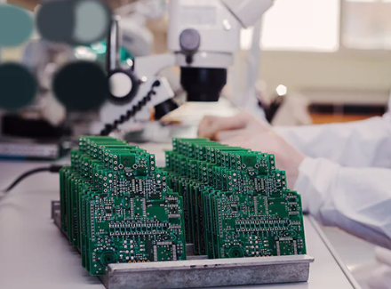
Rigorous inspection and testing protocols are indispensable in PCB assembly to ensure defect-free circuits and long-term reliability. After component placement and soldering, automated optical inspection (AOI) systems scan the PCBA for visible flaws, such as misaligned components, solder bridges, or insufficient solder joints. This non-contact method provides high-resolution imaging to detect deviations from design specifications early in the process. For hidden defects, X-ray inspection is employed to examine solder connections under ball grid array (BGA) packages or within multilayer boards, ensuring integrity in areas inaccessible to visual checks.
Electrical testing, including in-circuit testing (ICT), verifies the functionality of individual components and their connections by applying predefined voltage and signal patterns. This step identifies shorts, opens, or incorrect component values that could compromise performance. Functional testing further validates the assembled PCBA under real-world operating conditions, simulating power cycles, signal interactions, and load scenarios to confirm compliance with design requirements.
Environmental stress screening (ESS), such as thermal cycling or vibration tests, may also be integrated to assess durability under extreme conditions. These protocols not only minimize the risk of field failures but also align with industry standards like IPC-A-610 and ISO 9001. By combining automated and manual inspections, manufacturers can achieve a balanced approach to defect detection, optimizing yield rates while maintaining the high quality expected in modern PCB assembly workflows.
Thermal Management and Environmental Considerations
Effective thermal management is critical in PCB assembly to ensure long-term reliability and optimal circuit performance. During PCBA, components generate heat during operation, and inadequate dissipation can lead to overheating, reduced efficiency, or premature failure. Designers often integrate thermal vias, heatsinks, or thermally conductive materials to redirect heat away from sensitive components. For instance, using ceramic-filled substrates or metal-core PCBs enhances heat dissipation in high-power applications. Additionally, thermal simulation tools help predict hotspots, enabling proactive adjustments in component placement or layout before manufacturing.
Environmental factors also play a pivotal role in PCB assembly quality. Humidity, temperature fluctuations, and contaminants can compromise solder joints or corrode traces over time. To mitigate these risks, conformal coatings are applied post-assembly to protect boards from moisture, dust, and chemical exposure. Selecting coatings with appropriate properties—such as acrylic, silicone, or urethane—depends on the operating environment. For example, silicone coatings excel in high-temperature settings, while acrylics provide cost-effective moisture resistance.
Moreover, adhering to RoHS (Restriction of Hazardous Substances) and IPC standards ensures environmental compliance and minimizes ecological impact. Lead-free soldering, mandated by RoHS, reduces toxic waste but requires precise temperature control to maintain joint integrity. Manufacturers must also consider end-of-life recycling by using materials that align with WEEE (Waste Electrical and Electronic Equipment) directives.
In harsh environments, such as automotive or aerospace applications, PCBA undergoes rigorous testing under extreme temperatures, vibration, and humidity to validate durability. By addressing both thermal and environmental challenges early in the design phase, engineers can enhance the longevity and reliability of assembled PCBs, ensuring they meet performance expectations across diverse operating conditions.
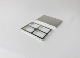
Final Assembly and Protective Coating Application
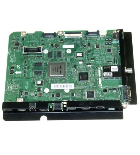
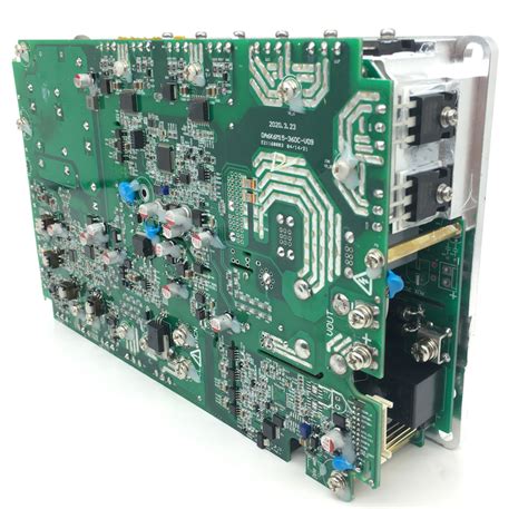
The final assembly stage in PCB assembly (PCBA) integrates mechanical components, such as connectors, enclosures, or heat sinks, with the populated board to complete the functional unit. This phase demands meticulous attention to alignment and secure fastening to avoid stress on solder joints or traces during operation. Once assembled, applying a protective coating is critical to safeguarding the board from environmental factors like moisture, dust, and chemical exposure. Conformal coatings—acrylic, silicone, or urethane-based—are commonly used to insulate components and prevent corrosion or short circuits. The coating process requires precision, as uniformity and complete coverage of high-risk areas (e.g., connectors, fine-pitch components) are essential for reliability.
Automated spray systems or selective coating techniques ensure controlled application, while manual methods like brushing may be employed for low-volume or rework scenarios. Post-coating, boards undergo curing under specific temperature and humidity conditions to achieve optimal adhesion and durability. Inspections, including visual checks or automated optical inspection (AOI), verify coating integrity and identify voids or uneven layers. For high-reliability applications, additional tests, such as thermal cycling or humidity resistance evaluations, validate the coating’s performance under stress.
By combining rigorous assembly practices with robust protective measures, PCBA manufacturers ensure the longevity and functionality of electronic systems, even in harsh operating environments. This step underscores the balance between mechanical robustness and environmental resilience in modern PCB assembly workflows.
Post-Assembly Quality Assurance and Compliance Checks
After completing the PCB assembly process, rigorous quality assurance (QA) and compliance checks are critical to ensure the reliability and performance of the final PCBA (Printed Circuit Board Assembly). These steps validate that the board meets both functional specifications and industry standards. Visual inspections are typically the first line of defense, where technicians use magnification tools to identify soldering defects, such as bridges, cold joints, or misaligned components. For higher precision, automated systems like Automated Optical Inspection (AOI) scan the board against design files to flag discrepancies in component placement or soldering quality.
Advanced X-ray inspection is employed for hidden connections, such as those in Ball Grid Arrays (BGAs), to detect voids or cracks in solder joints that are invisible to the naked eye. Functional testing follows, where the assembled board is powered and subjected to simulated operating conditions. This step verifies electrical performance, signal integrity, and compatibility with connected systems. Environmental stress tests, including thermal cycling and vibration testing, assess the PCBA’s durability under extreme temperatures or mechanical shocks, ensuring it can withstand real-world applications.
Compliance with industry standards, such as IPC-A-610 (for acceptability of electronic assemblies) and ISO 9001 (quality management systems), is mandatory for many applications. Certifications like RoHS and REACH are also validated to confirm adherence to environmental regulations. Documentation, including test reports and traceability records, is meticulously maintained to facilitate audits and future troubleshooting. By integrating these checks, manufacturers minimize defects, reduce field failures, and deliver PCB assemblies that consistently meet performance and regulatory expectations.
Conclusion
The journey of PCB assembly (often abbreviated as PCBA) culminates in a meticulous synthesis of technical precision and rigorous validation to ensure optimal circuit performance. Every phase, from design verification and component placement to advanced soldering and thermal management, plays a pivotal role in achieving reliability. Modern PCBA processes demand adherence to automated inspection protocols and environmental stress testing to identify defects early, minimizing failures in real-world applications. Protective coatings, such as conformal finishes, further safeguard assemblies against moisture, dust, and temperature fluctuations, extending operational lifespans. Post-assembly, quality assurance steps like functional testing and compliance audits validate that the final product meets industry standards, from signal integrity to power efficiency. By integrating these essential steps, manufacturers not only enhance the durability of PCB assemblies but also ensure they perform consistently under diverse conditions. Ultimately, a well-executed PCBA workflow bridges the gap between theoretical design and practical functionality, delivering circuits that power today’s advanced electronics with precision.
FAQs
What distinguishes PCB assembly from PCBA?
PCB assembly refers to the process of attaching electronic components to a bare circuit board, while PCBA (Printed Circuit Board Assembly) denotes the completed board with all components mounted and tested. Both terms are often used interchangeably, but PCBA emphasizes the fully functional end product.
How does component placement accuracy impact circuit performance?
Precise component placement ensures proper electrical connectivity and minimizes signal interference. Automated pick-and-place machines achieve micron-level accuracy, critical for high-density designs. Misaligned components can lead to short circuits, thermal imbalances, or complete circuit failure.
Why are soldering methods vital in PCB assembly?
Advanced techniques like reflow soldering and wave soldering create durable electrical connections. Reflow is ideal for surface-mount devices (SMDs), while wave soldering suits through-hole components. Poor soldering can cause cold joints or cracked connections, compromising reliability.
What inspection protocols detect defects post-assembly?
Automated Optical Inspection (AOI) and X-ray imaging identify soldering flaws, misaligned components, or voids. Electrical testing, including in-circuit testing (ICT) and functional testing, validates performance under simulated operating conditions.
How does thermal management affect long-term reliability?
Effective heat dissipation through thermal vias, heatsinks, or conductive pads prevents component degradation. Overheating accelerates electromigration in traces, leading to premature failure. Designs must balance power density with cooling solutions.
What role do protective coatings play in PCBA?
Conformal coatings shield assemblies from moisture, dust, and chemical exposure. Materials like acrylic or silicone enhance durability in harsh environments. Coatings also reduce risks of corrosion and electrical leakage.
Which compliance standards apply to PCB assembly?
Certifications like IPC-A-610 (acceptability of electronic assemblies) and ISO 9001 ensure quality consistency. Compliance with RoHS and REACH regulations guarantees adherence to environmental and safety guidelines.
How are environmental factors addressed during assembly?
Controlled humidity and temperature in production areas prevent oxidation and solder paste degradation. Electrostatic discharge (ESD) safeguards protect sensitive components from static damage during handling.
Ready to Optimize Your PCB Assembly Process?
For tailored solutions in high-performance PCB assembly and PCBA services, please click here to explore advanced manufacturing capabilities tailored to your project’s needs.