Ground interference and the influence of PCB routing
Ground interference and the influence of PCB routing are important and complex issues in circuit design. The following is a detailed analysis and summary of these two issues:
I feel that the requirements for audio are a little higher, so I will share it here and talk about audio later:
1.Ground interference
Ground interference refers to signal interference generated by a common ground wire, which usually occurs between different unit circuits, components or systems. The forms of ground interference can be mainly classified into three categories:
Ground loop interference: Due to the existence of ground impedance, when current flows through the ground wire, a voltage will be generated on the ground wire. When the current is large, this voltage can be very large. For example, when a high-power electrical appliance is started nearby, a strong current will flow through the ground wire, thereby generating a differential mode voltage in the “ground loop”, which affects the circuit.
Common impedance interference: When two circuits share a ground wire, due to the impedance of the ground wire, the ground potential of one circuit will be modulated by the working current of the other circuit. This coupling is called common impedance coupling, which may cause the signal to couple from one circuit to another.
Ground loop electromagnetic coupling interference: On the PCB of the actual circuit, the “ground loop” will surround a certain area. According to the law of electromagnetic induction, this loop will generate an electromagnetic field, which will be electromagnetically coupled with nearby wires, thereby causing interference.
2.The impact of PCB routing
The impact of PCB routing on circuit performance is mainly reflected in the following aspects:
Wire impedance: The wires (including ground wires) on the PCB also have impedance. For AC signals, the inductive reactance component of the wire cannot be ignored, especially when the frequency is high. This impedance may cause problems such as signal attenuation and phase shift.
Signal crosstalk: When the routing layout on the PCB is unreasonable, crosstalk may occur between different signal lines. This may be caused by capacitive coupling, inductive coupling or electromagnetic radiation between signal lines.
Electromagnetic interference (EMI): Factors such as routing layout, line width, and line spacing on the PCB may affect the size of electromagnetic interference. Unreasonable routing layout may lead to increased electromagnetic radiation, thereby interfering with other circuits or systems.
In order to reduce the influence of ground interference and PCB routing, the following measures can be taken:
Optimize ground design: minimize ground impedance, avoid ground loops, use multilayer board design to separate grounds of different voltages, etc.
Rationally layout PCB routing: avoid crossing and overlapping between signal lines, maintain sufficient line spacing and line width, use shielding wires or ground wires to isolate sensitive signals, etc.
Use filters, isolators and other devices to reduce interference: These devices can effectively filter out or isolate interference signals and improve the anti-interference ability of the circuit.
Due to stray currents in the ground circuit, unnecessary potentials may accumulate in other sensitive locations, so the ground is not truly zero potential, that is, the potential is increased. To prevent this from happening, a variety of techniques can be used, including the following measures:
Do not bundle the signal return trace and the power return trace directly together; 2. Separate the power ground and signal ground, as shown;
Use a ground plane, as shown;
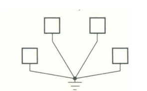
Apply a star ground/single point ground configuration, as shown:
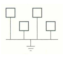
Use a ground bus, as shown:
For differential mode interference signals introduced by the grounded power system, especially in the over-standard frequency bands of 9kHz~5MHz and 30~70MHz, the following are some recommended treatment methods:
Use Y2 capacitors:
On the L line and N line, that is, the live line and the neutral line, each connect a Y2 capacitor in series to the ground. The Y2 capacitor is a type of safety capacitor, mainly used to bridge the L line, N line and the ground, and its function is to suppress common mode interference. But here, it can also have a certain inhibitory effect on differential mode interference, especially in specific frequency bands.
Introducing differential mode inductors:
Before the ground wire is connected to the power system, it first passes through a differential mode inductor. The differential mode inductor is mainly used to suppress differential mode interference on the power line. It allows the power current to pass, but produces a large impedance to the differential mode interference current, thereby suppressing the differential mode interference.
Using nickel-zinc magnetic rings:
The ground wire is covered with a nickel-zinc magnetic ring and wound 2 to 4 times. The nickel-zinc magnetic ring has a high magnetic permeability and magnetic saturation sense, and can absorb high-frequency noise and interference signals. By winding a certain number of turns, its suppression of interference in a specific frequency band can be enhanced.
Similarly, the output line can also be covered with a nickel-zinc magnetic ring and wound 2 to 4 times to reduce the interference signal on the output line.
In terms of power ground, the three common main power loops in the drive include:
PFC power loop:
Used to improve the power factor of the power supply and reduce harmonic pollution to the power grid.
DC-DC power loop (buck, flyback, forward, half-bridge, full-bridge, etc.):
These are DC to DC conversion circuits used to convert one DC voltage to another DC voltage to meet the needs of different circuits or devices.
Output power loop:
This refers to the loop in which the power supply provides power to the load, which directly determines the output performance and stability of the power supply.
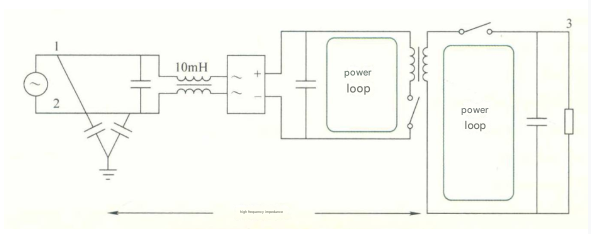
The power loop in the flyback converter is shown in the figure:
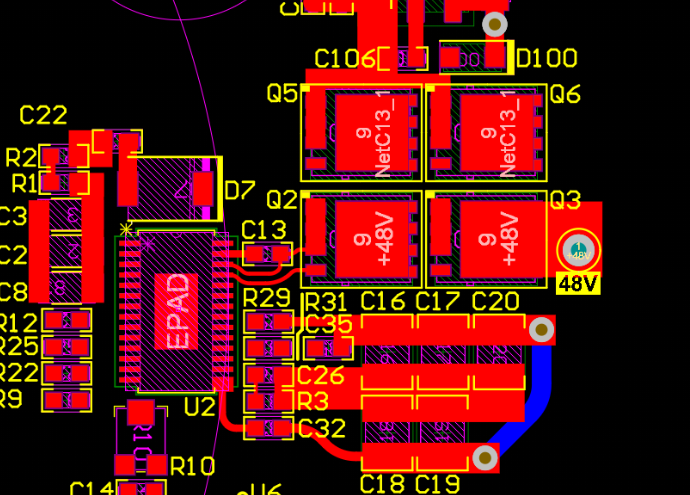
In the power loop design, the treatment of the ground trace is crucial to prevent interference and ensure circuit performance. The following is a detailed analysis and suggestions for the treatment of the ground trace in the power loop based on the information you provided and the relevant content in the reference article:
The importance of ground traces in the power loop
Prevent signal traces from being interfered with: There may be large current changes (di/dt) in the power traces, which will generate electromagnetic fields and interfere with nearby signal traces. Therefore, the ground traces of the power loop must be separated from the signal ground traces to reduce this interference.
Reduce loop routing area: Too large loop routing area will increase the possibility of electromagnetic radiation, especially in the 30~50MHz and 70~100MHz frequency bands. Therefore, it is an effective way to reduce electromagnetic radiation to reasonably design the loop routing of the power ground and reduce its area.
Correction method
Add a small MLCC capacitor between the DS of the PFC MOSFET:
Add a small MLCC (multilayer ceramic capacitor) capacitor between the drain (D) and source (S) of the MOSFET, with a capacitance between 22~100pF. Too small a capacitor has little effect, while too large a capacitor may lead to reduced efficiency and excessive temperature rise of the MOSFET.
If space permits, it is recommended to use plug-in ceramic capacitors instead of high-voltage MLCCs, as they generally have better performance.
Connect an RC circuit in parallel to the topological diode of the PFC:
For small and medium power converters, an RC circuit can be connected in parallel to the topological diode, where R is around 100Ω and C is below 100pF. This method can significantly reduce electromagnetic radiation, but it may affect efficiency and require re-adjustment of related parameters.
It should be noted that the addition of the RC circuit may affect the zero-crossing detection function of some APFC chips, such as ST’s L6562X series chips. Therefore, it needs to be used with caution in actual applications and necessary debugging should be performed.
For the topology structure of the Flyback connected to the PFC back stage:
If the PFC back stage is connected to the Flyback topology, the above method can still be used to add MLCC small capacitors and RC circuits to the MOSFET and topology diode to reduce electromagnetic radiation.