High-speed PCB design software stacking structure design suggestions
When designing a multi-layer PCB, the number of PCB layers depends on the complexity of the circuit board. From the perspective of the PCB processing process, a multi-layer PCB is manufactured by stacking and pressing multiple “double-sided PCBs”, but the number of layers of the multi-layer PCB, the stacking order between the layers and the selection of the board material are determined by the circuit board designer. This is the so-called “PCB stacking design”.
Text
As the saying goes, the best practice is also based on theoretical knowledge. In this section, Banermei focuses on sharing with you the conceptual theoretical knowledge of PCB stacking design and the design suggestions for the stacking structure.
1.The composition of PCB stacking
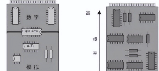
The layer settings in the PCB design file include the following: silk screen layer, solder mask layer, wiring layer, and plane layer.
Silk Screen: It is the physical layer where the device description information and board name identification are placed in the PCB board.
Soldermask: Soldermask is an important part of PCB, which mainly plays the role of solder resistance and environmental protection. Soldermask is a layer of ink attached to the surface of PCB. Its function is to cover the PCB area that does not need soldering, prevent tinning, and protect the circuit from external damage to a certain extent.
Conductor: It is a physical layer that realizes the interconnection relationship between various devices on the PCB board in a “positive film” manner.
Plane: It is a physical layer that realizes the connection of various power supplies and ground networks on the PCB board and provides impedance reference and return path.

2.Design suggestions for stacked structure
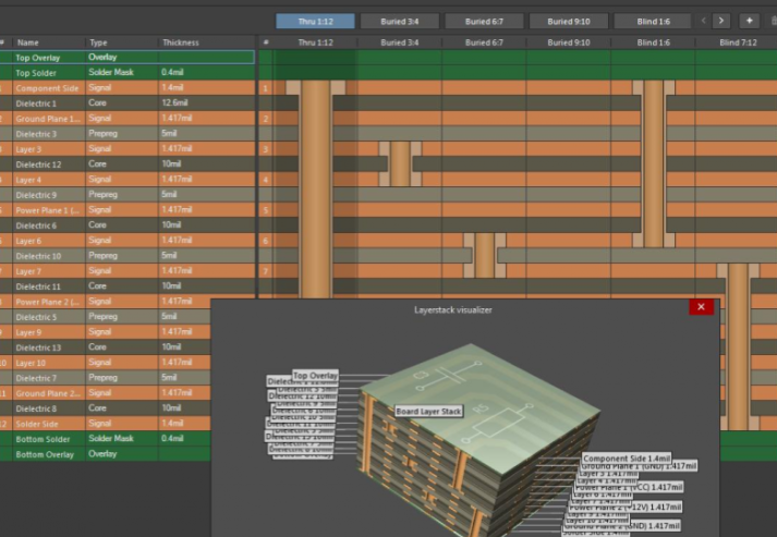
The “stacked design” usually refers to the design of the stacking arrangement of the wiring layer and the plane layer.
The recommended PCB stacking method is Foil stacking.
- Minimize the use of PP sheets and CORE models and types in the same stacking (no more than 3 PP stacking layers per layer of medium).
- The thickness of PP medium between two layers should not exceed 21MIL (thick PP medium is difficult to process, and generally a core board will be added, resulting in an increase in the actual number of stacking layers, thereby increasing the processing cost).
- The outer layer (Top and Bottom layer) of PCB generally uses 0.5OZ thick copper foil, and the inner layer generally uses 1OZ thick copper foil.
Note: The thickness of the copper foil is generally determined according to the current size and the thickness of the trace. For example, the power board generally uses 2-3OZ copper foil, and the ordinary signal board generally chooses 1OZ copper foil. In the case of thin traces, 1/3QZ copper foil may be used to improve the yield rate; at the same time, avoid using core boards with inconsistent copper foil thickness on both sides in the inner layer. - The distribution of the wiring layer and the plane layer of the PCB board requires symmetry from top to bottom from the center line of the PCB board stacking (including the number of layers, the distance from the center line, the copper thickness of the wiring layer, etc.)
Note: The PCB stacking method needs to adopt a symmetrical design. The symmetrical design means that the thickness of the insulation layer, the type of prepreg, the thickness of the copper foil, and the type of graphic distribution (large copper foil layer, line layer) should be as symmetrical as possible relative to the center line of the PCB. - The design of line width and dielectric thickness needs to leave sufficient margin to avoid design problems such as SI caused by insufficient margin.
In a small number of PCB designs, wiring is done on the power ground plane layer or the power and ground network is done on the wiring layer. This type of mixed layer design is uniformly called the signal layer.
In summary, before designing a multi-layer PCB, the layout engineer needs to determine the circuit board structure to be used based on the scale of the circuit, the size of the circuit board, and the requirements of electromagnetic compatibility, that is, to decide whether to use a 4-layer, 6-layer, or more-layer circuit board.