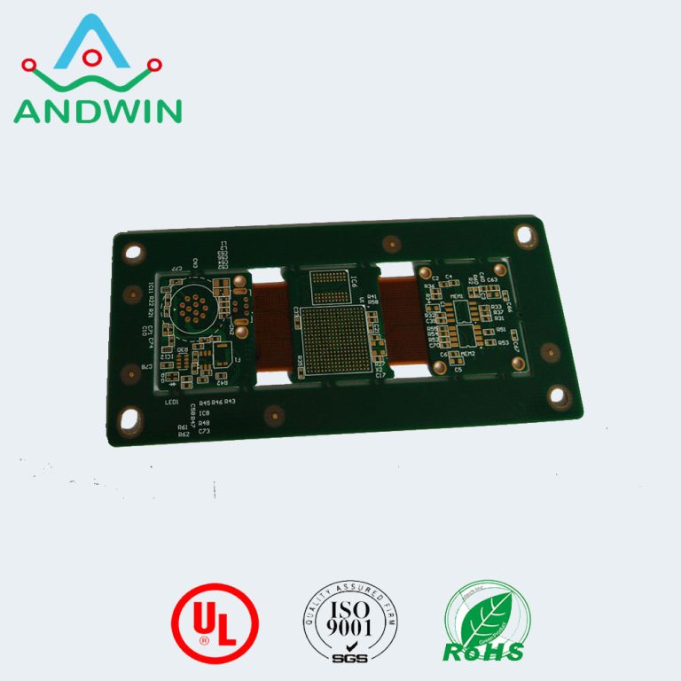
High speed pcb routing
1. Differential pair routing:
This involves routing two signals that are equal in magnitude and opposite in polarity,
which helps to reduce electromagnetic interference (EMI) and improve signal integrity.
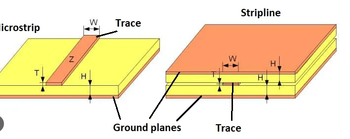
2. Controlled impedance routing:
This involves designing the PCB with specific trace widths and spacing to achieve a desired impedance,
which helps to minimize signal reflections and distortion.
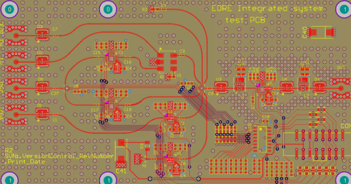
3. Via placement:
The placement of vias can have a significant impact on signal quality,
so careful consideration is given to their location and spacing.
4. Signal layer stackup:
The arrangement of signal and ground planes in the PCB stackup can also affect signal quality,
so designers may use specific layer configurations to minimize noise and crosstalk.
Overall, high speed PCB routing requires a deep understanding of signal transmission and PCB design principles,
as well as specialized software tools and simulation techniques to ensure optimal performance.
~~(%WW3QW]T7K]`_L]Q0")
High speed PCB routing refers to the process of designing and routing printed circuit boards (PCBs) that are optimized for high speed signal transmission.
This involves careful consideration of factors such as signal integrity, impedance matching, and noise reduction.
the role of high speed pcb routing
High speed PCB routing plays a crucial role in ensuring the proper functioning of electronic devices that require high-speed data transfer rates.
It involves designing the layout of printed circuit boards (PCBs) in a way that minimizes signal loss and interference,
while maximizing signal integrity and reliability.
High-speed PCB routing is essential for applications such as telecommunications, data centers, and high-performance computing,
where data transfer rates are critical.
It involves the use of specialized techniques and tools to ensure that signals are transmitted at the required speed and with minimal distortion.
Some of the key factors that need to be considered in high-speed PCB routing include the impedance of the transmission lines,
the placement of vias and components, the routing of power and ground planes, and the use of appropriate termination techniques.
Overall, the role of high-speed PCB routing is to ensure that electronic devices can operate at their maximum potential,
with fast and reliable data transfer rates that meet the needs of modern applications.
high speed pcb design training in bangalore
There are several institutes and training centers in Bangalore that offer courses on high speed PCB design. Some of them are:
1. Vector Institute:
This institute offers a course on high speed PCB design using Altium Designer software.
The course covers topics such as signal integrity, power integrity, high speed routing, and EMI/EMC considerations.
2. EDA Direct:
This training center provides courses on PCB design using various software tools such as Altium Designer, OrCAD, and Allegro.
The courses cover topics such as high speed design, analog and mixed signal design, and PCB layout.
3. Mentor Graphics:
This company offers training courses on PCB design using their software tools such as PADS and Xpedition.
The courses cover topics such as high speed design, signal integrity, power integrity, and thermal analysis.
4. Cadence Design Systems:
This company offers training courses on PCB design using their software tools such as Allegro and OrCAD.
The courses cover topics such as high speed design, signal integrity, power integrity, and thermal analysis.
5. VLSI Guru:
This institute offers a course on high speed PCB design using Altium Designer software.
The course covers topics such as signal integrity, power integrity, high speed routing, and EMI/EMC considerations.
These are some of the institutes and training centers in Bangalore that offer courses on high speed PCB design.
You can choose the one that best suits your requirements and budget.