How PCB Suppresses the Propagation of Electromagnetic Interference (EMI)
Printed circuit boards (PCBs) are easy to manufacture, reliable in performance, and cheap, so they are widely used in various electronic devices. In recent years, with the development of electronic technology, the clock rate in microprocessors and logic circuits on printed circuit boards has become faster and faster, and the rise/fall time of signals has become shorter and shorter. At the same time, the density of devices and wiring on the board has continued to increase, and the electromagnetic compatibility problem of printed circuit boards has become increasingly prominent.
When analyzing printed circuit boards at the electromagnetic compatibility level, three basic issues should be considered:
Ensure reliable transmission of signals on the board to ensure signal integrity (Signal Integrity);
Suppress the propagation of electromagnetic interference EMI;
Strengthen protection to prevent sensitivity failures (Susceptibility Failure) caused by insufficient anti-interference.
For relatively low-frequency signals (the upper limit of the signal spectrum is 100MHz), the above issues can usually be ignored.
However, when the signal wavelength (λ) and the signal line length (l) are comparable (l ≥ 0.1λ), it is necessary to consider the geometric dimensions of the printed line, wiring, line spacing, rise and fall time of the transmission signal, pulse width and period, etc., so that the transmission line theory (microwave theory is needed in some cases) is needed to correctly analyze the propagation of the signal.
The printed lines on the printed circuit board can usually be simulated by microstrip or stripline models.
The microstrip model consists of a conductor strip on one side of the dielectric substrate and a metal ground plate on the other side of the substrate. It can be used to simulate the printed wires on the surface layer of the PCB. The stripline model consists of upper and lower ground conductors and an intermediate conductor strip. There is an insulating medium between the ground plate and the conductor strip. It can simulate the printed wires in the middle layer of a multi-layer PCB.
1.Signal integrity
The signal integrity problems on the PCB mainly include delay, impedance mismatch, ground bounce, crosstalk, etc. Signal integrity problems will affect the stable operation of electronic devices.
(1) Signal delay: For high-frequency signals, transmission delay should be one of the most basic issues that circuit designers consider. The relationship between transmission delay and the length of the signal line and the signal transmission speed is as follows:
Where: c is the speed of light in a vacuum;
εreff is the effective relative conductivity;
lp is the length of the signal line.
εreff is related to the medium around the transmission line. For microstrip transmission lines, ε is between the relative conductivity of the board and the relative conductivity of air. In most systems, the length of the signal transmission line is the most direct factor affecting the clock pulse phase difference (colock skew). The clock pulse phase difference refers to the time when two clock signals generated at the same time arrive at the receiving end. The clock pulse phase difference reduces the predictability of the arrival of the signal edge. If the clock pulse phase difference is too large, an erroneous signal will be generated at the receiving end, as shown in Figure 1. Transmission line delay has become an important part of the clock pulse cycle (Clock Cycle).
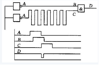
Figure 1 Effect of transmission delay on signal
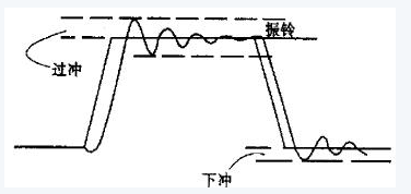
Figure 2 Ringing phenomenon caused by reflection
(2) Impedance mismatch:
Impedance mismatch can be caused by the different impedances of the driving source, transmission line and load, or by discontinuity of the transmission line? For example, vias, short stubs? In addition, due to the change of local inductance and capacitance on the return path, discontinuity of the return path will also lead to impedance discontinuity. This impedance mismatch will lead to reflection and damped oscillation. Reflection will cause signal ringing? Ringing? phenomenon, that is, voltage overshoot and undershoot generated above and below the steady-state signal, as shown in Figure 2. In order to limit the voltage overshoot/undershoot within a reasonable range (not exceeding 10% to 15% of the steady-state value), the following principle should be followed: the rise time of the signal should be less than the transmission delay caused by the signal going back and forth on the printed conductor. That is: tr≤2lp/tppd
Where: tr—refers to the rise time of the signal;
lp—the length of the signal line;
tppd—the delay caused by the unit length of the signal line.
Ringing may cause false triggering. To eliminate the influence of ringing, one method is to wait for the signal to stabilize, but this will reduce the maximum possible clock rate of the system.
(3) Ground Bounce:
Ground bounce refers to the fact that when a certain integrated circuit is switched, the ground line of the PCB and the ground lead of the integrated circuit have a certain inductance, which will cause a brief impact or drop in the ground potential inside the device. The input drive signal from other devices, or other devices driven by the output signal of this device, are all referenced to the external system ground. This inconsistency in the reference ground potential may cause changes in the input threshold or output level of the device, thereby causing problems in the design of high-speed PCBs. Similar problems also exist for power supplies.
(4) Crosstalk:
It can usually be divided into two parts, namely common impedance coupling and electromagnetic field coupling. Common impedance coupling is caused by different signals sharing a common return path. This coupling usually plays a decisive role at low frequencies. Electromagnetic field coupling can be divided into inductive coupling and capacitive coupling. Crosstalk is a near-field problem. On PCB0, crosstalk is related to the length of the line, the spacing between the lines, the direction of the signal transmitted in the line, and the condition of the reference ground plane. For example, a crack on the ground plane will increase the crosstalk of the adjacent lines across the crack, causing signal waveform distortion.
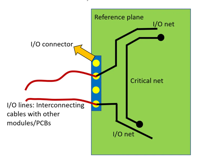
2 Reduce conducted interference and radiated interference
Electromagnetic interference problems mainly include conducted interference and radiated interference. The so-called interference in electromagnetic compatibility refers to the “phenomenon of electromagnetic energy being emitted from the source to the outside”. Unlike the artificial outward electromagnetic waves in the general communication field, the interference in PCB is often unintentional. The radiated interference standard usually covers the range of 30MHz~1GHz, and will be extended to 5~40GHz in the near future. For conducted interference, FC limits the range to 0.45~30MHz, while CISPR extends the lower limit to 0.15MHz. Filtering is an important method to suppress conducted interference. Filtering the signal lines leaving the PCB board can suppress the propagation of conducted radiation.
At high frequencies, the printed lines on the PCB act like monopole antennas or loop antennas, radiating energy outward. Radiated radiation can be divided into two basic types: differential mode radiation and common mode radiation.
Differential mode radiation is caused by the current in the closed loop? The so-called differential mode current?. The intensity of the radiation is proportional to the area of the loop, the magnitude of the current and the square of the frequency. By reducing the above factors, especially the frequency, the intensity of the radiation can be reduced. In addition, the radiation of the loop is directional, and the electric field radiation value of a small current loop is the largest in the plane where the loop is located, and the smallest in the axial direction of the loop.
Common mode radiation is caused by parasitic effects, such as induced currents in the ground layer, power layer or cable? The so-called common mode current?. Common mode radiation is similar to a monopole antenna. The intensity of the radiation is related to the current and frequency per unit line length, but it is not sensitive to direction.
Since the radiation generated by differential mode current is subtractive, while the radiation generated by common mode current is additive, even if the common mode current is much smaller than the differential mode current, it will generate a radiation field of comparable degree. For example, a cable with a length of 1m and a differential mode current of 30MHz and 20mA flowing in two conductors with a spacing of 1.27mm will generate a radiation electric field of 100μV/m at a distance of 3m, while for common mode current, only 8μA of current is needed to generate the same degree of radiation. When performing far-field analysis, common mode radiation must be considered.
3 Strengthen protection
The intensity of protection depends on the purpose of the product. For insignificant electronic products, no special protection is required. For military electronic products and electronic equipment used for power plant and power grid control, the highest level of protection is required, because even in extreme cases, these devices must be guaranteed to work properly.
4 Conclusion
When designing printed circuit boards, electromagnetic compatibility issues must be considered to ensure the realization of design functions. At high frequencies, simple circuit simulation may no longer be applicable, and transmission line theory or microwave theory may be needed to analyze the problems encountered.