How should the components of high-speed PCB be laid out?
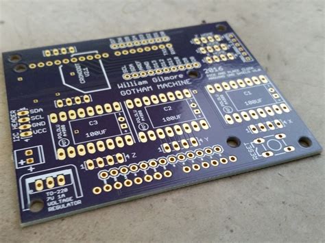
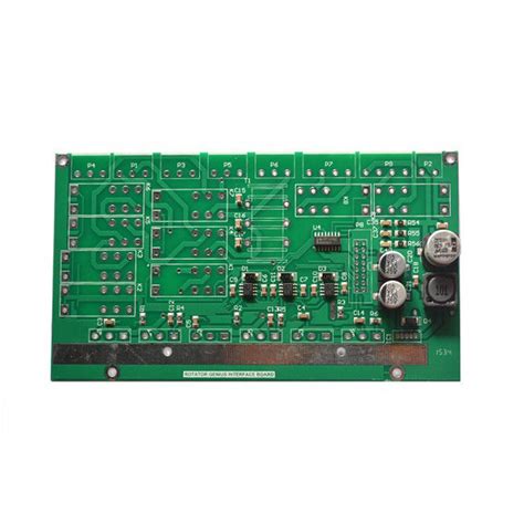
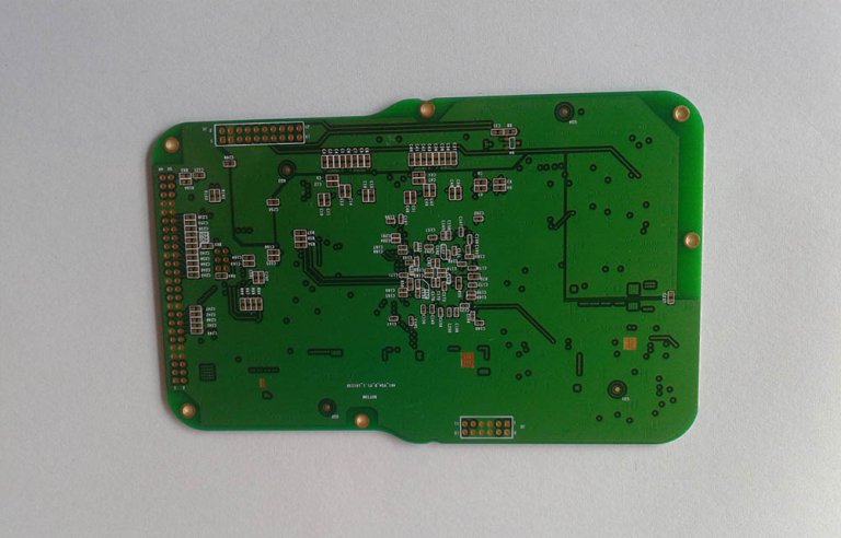
After determining the material, stacking design, size, and overall partition concept of the PCB, it is necessary to lay out the components, specifically, to place all components in appropriate positions on the PCB. A good component layout can enhance the electromagnetic compatibility of the PCB and is also a prerequisite for good wiring.
When laying out all the components of the circuit according to the functional units of the circuit, the following principles must be met:
· According to the flow direction of the circuit and the position of each functional circuit unit, the layout should be suitable for signal flow, and the signal should be kept in the same direction as much as possible;
· The core components of each functional circuit are the center, and the layout is carried out around this center. The components should be arranged evenly, neatly, and compactly on the PCB, and the leads and connections between the components should be simplified as much as possible;
· For circuits working at high frequencies, the distribution parameters between components should be considered. In general, the components should be arranged in parallel as much as possible in the circuit. In this way, it is not only beautiful, but also easy to install and weld, and easy to mass produce;
· The components located at the edge of the circuit board are generally not less than 2 mm away from the edge of the circuit board;
· The position occupied by the positioning holes and fixing brackets of the printed circuit board should be reserved.
When laying out special components, the following issues should also be noted:
· Try to shorten the connection between high-frequency components as much as possible, and try to reduce their distributed parameters and mutual electromagnetic interference. Components susceptible to interference should not be too close to each other, and input and output components should be kept as far away as possible;
· Some components or wires may have a high potential difference, and the distance between them should be increased to avoid discharge leading to accidental short circuits. Components with high voltage should be placed in places that are difficult to reach during debugging;
· Components weighing more than 15 g should be fixed with a bracket and then welded. Those heavy and large components that generate a lot of heat should not be installed on the printed circuit board, but should be installed on the chassis bottom plate of the whole machine, and heat dissipation should be considered.
Thermistors should be kept away from heating components;
· The layout of adjustable components such as potentiometers, adjustable inductors, variable capacitors, and micro switches should consider the structural requirements of the whole machine. If it is adjusted inside the machine, it should be placed in a convenient place on the printed circuit board for adjustment; if it is adjusted outside the machine, its position should be consistent with the position of the adjustment knob on the chassis panel.