How to Plan the Number of PCB Routing Layers Effectively
Introduction
Printed Circuit Board (PCB) design is a complex process that requires careful consideration of numerous factors, with the number of routing layers being one of the most critical decisions. The layer count directly impacts the board’s performance, manufacturability, cost, and reliability. This 2000-word article provides a comprehensive guide on how to effectively plan the number of routing layers for your PCB design, covering key considerations, methodologies, and best practices.
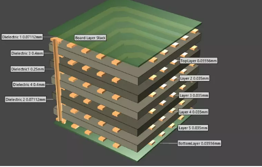
Understanding PCB Layer Basics
Layer Composition in Modern PCBs
A typical PCB consists of several types of layers:
- Signal layers: For component interconnection
- Power planes: For power distribution
- Ground planes: For return paths and shielding
- Dielectric layers: Insulating material between conductive layers
Common PCB Layer Configurations
PCBs range from simple single-layer boards to complex multilayer configurations:
- Single-layer (1L)
- Double-layer (2L)
- 4-layer
- 6-layer
- 8-layer
- 10-layer or more (for high-density designs)
Key Factors Influencing Layer Count Decisions
1. Circuit Complexity and Component Density
The number of components and their interconnection requirements primarily determine the necessary routing layers. High-density designs with complex ICs (BGAs, QFNs) typically require more layers to accommodate all connections.
2. Signal Integrity Requirements
High-speed designs demand careful consideration:
- Controlled impedance routing
- Proper return paths
- Minimized crosstalk
- Reduced electromagnetic interference (EMI)
More layers allow for better isolation between signal types and implementation of proper reference planes.
3. Power Distribution Needs
Complex power systems may require:
- Multiple voltage rails
- Clean power isolation
- Low-impedance power delivery networks
Additional power planes can significantly improve power integrity.
4. Thermal Management Considerations
High-power designs benefit from:
- Dedicated thermal layers
- Proper heat dissipation paths
- Copper balancing
5. Manufacturing Constraints and Cost Factors
Each additional layer increases:
- Board fabrication cost
- Production time
- Potential yield issues
Finding the optimal balance between performance and cost is essential.
Methodology for Determining Layer Count
Step 1: Initial Estimation Based on Component Count
Use these rough guidelines:
- Low density (100-200 pins): 2 layers may suffice
- Medium density (200-500 pins): 4 layers recommended
- High density (500-1000 pins): 6-8 layers
- Very high density (1000+ pins): 8+ layers
Step 2: Pin Density Calculation
A more precise method uses pin density:
Pin density = (Number of components × Average pins per component) / Board area (in²)- <20 pins/in²: 2 layers
- 20-50 pins/in²: 4 layers
- 50-100 pins/in²: 6 layers
- 100-160 pins/in²: 8 layers
- >160 pins/in²: 10+ layers
Step 3: Signal Type Analysis
Account for different signal types:
- High-speed signals (require controlled impedance)
- Analog signals (need isolation)
- RF signals (demand special considerations)
- Power signals (thicker traces or planes)
Step 4: Power Delivery Network (PDN) Requirements
Evaluate:
- Number of voltage rails
- Current requirements
- Noise sensitivity
Each significant voltage rail may need its own plane or large copper pour.
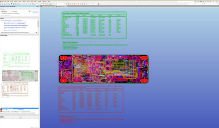
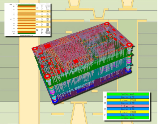
Step 5: Stackup Planning
Develop a preliminary stackup considering:
- Signal layer distribution
- Plane layer placement
- Dielectric materials
- Impedance control requirements
Optimizing Layer Usage
Efficient Routing Strategies
- Layer Orientation: Alternate horizontal and vertical routing directions
- Via Minimization: Reduce layer transitions
- Area Routing: Utilize all available space efficiently
- Bus Routing: Group related signals
Layer Assignment Best Practices
- Place critical signals adjacent to reference planes
- Group similar signal types together
- Separate noisy and sensitive signals
- Use buried layers for critical routing
Power and Ground Planning
- Dedicate entire layers to power and ground when possible
- Implement split planes carefully to avoid creating antennas
- Maintain continuous return paths for high-speed signals
Common Layer Configurations and Their Applications
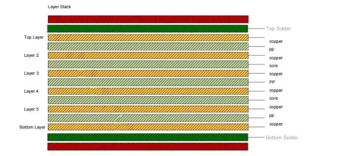
4-Layer Stackup
Typical arrangement:
- Top (components and signals)
- Ground plane
- Power plane
- Bottom (components and signals)
Best for: Medium complexity designs, good signal integrity at reasonable cost
6-Layer Stackup
Common configurations:
- Top
- Ground
- Signal
- Signal
- Power
- Bottom
Or:
- Top
- Signal
- Ground
- Power
- Signal
- Bottom
Best for: Higher complexity, better signal isolation, improved power delivery
8-Layer Stackup
High-performance arrangement:
- Top
- Ground
- Signal
- Power
- Ground
- Signal
- Power
- Bottom
Best for: Complex designs with multiple power rails and critical signal integrity requirements
Advanced Considerations
High-Speed Design Implications
For designs with signals above 50MHz:
- Maintain consistent reference planes
- Implement proper termination
- Control impedance throughout the signal path
- Consider differential pair routing requirements
EMI Reduction Techniques
- Use ground layers to shield sensitive signals
- Implement proper stitching vias
- Maintain continuous return paths
- Consider edge shielding requirements
Manufacturing Tolerances
Account for:
- Minimum trace width/spacing
- Via size and type limitations
- Layer registration tolerances
- Material properties and consistency
Cost Optimization Strategies
Right-Sizing the Layer Count
- Avoid over-engineering but don’t underestimate requirements
- Consider future expansion needs
- Evaluate cost vs. performance tradeoffs
Panel Utilization
- Standard layer counts often have better pricing
- Odd layer counts may require special processing
- Consider board thickness constraints
Alternative Approaches
- Higher density routing (smaller traces/spaces)
- Advanced via technologies (microvias, buried vias)
- Component placement optimization
Design Tools and Automation
PCB Design Software Features
Modern EDA tools offer:
- Layer count estimation
- Routing completion analysis
- Signal integrity simulation
- Power distribution network analysis
Using Autorouters Effectively
- Set appropriate constraints
- Define layer directions and priorities
- Balance autorouter use with manual routing
Verification and Validation
Design Rule Checking (DRC)
- Verify layer-specific constraints
- Check plane continuity
- Validate spacing rules
Signal Integrity Analysis
- Perform pre-layout and post-layout simulations
- Verify impedance control
- Analyze crosstalk and EMI
Prototyping and Testing
- Build test vehicles for critical designs
- Measure actual performance
- Iterate if necessary
Future Trends and Considerations
High-Density Interconnect (HDI) Technologies
- Finer features enabling more routing in fewer layers
- Advanced via structures
- Sequential lamination techniques
Embedded Components
- Potential to reduce surface routing needs
- Improved signal integrity for certain components
Flexible and Stretchable PCBs
- Unique layer planning requirements
- Different material considerations
Conclusion
Planning the appropriate number of PCB routing layers requires careful analysis of technical requirements, performance objectives, and cost constraints. By following a systematic approach that considers component density, signal types, power needs, and manufacturing realities, designers can arrive at optimal layer counts that balance all these factors. Remember that while adding layers can solve many design challenges, each additional layer increases cost and complexity—the art of PCB layer planning lies in finding the sweet spot that meets all requirements without unnecessary overhead.
As PCB technology continues to evolve with higher densities and more advanced materials, the methodologies for determining layer counts will also progress. However, the fundamental principles outlined in this article will remain relevant for creating efficient, reliable, and cost-effective PCB designs across various applications and industries.