
How to set up the right shielding for PCB layers?
In product development, it is usually better to carefully consider and implement the right design early in the project development cycle from a cost, schedule, quality and performance perspective. Add-ons and other “quick” fixes implemented late in the project are usually non-ideal solutions in terms of functionality, have poor quality and reliability, and cost more than if implemented earlier in the process.
Lack of foresight in the early design stages of a project often leads to delayed delivery and can result in a dissatisfied customer.
This problem applies to any design, whether analog, digital, electrical, mechanical, etc. Shielding an entire PCB costs about 10 times more than shielding individual ICs and parts of the PCB, and 100 times more to shielding the entire product. If an entire room or building needs to be shielded, the costs are truly astronomical.
In product development, it is usually better to carefully consider and implement the right design early in the project development cycle from a cost, schedule, quality and performance perspective.
Add-ons and other “quick” fixes implemented late in the project are usually non-ideal solutions in terms of functionality, have poor quality and reliability, and cost more than if implemented earlier in the process. Lack of foresight in the early design phases of a project often leads to delayed delivery and potentially unhappy customers. This problem applies to any design, whether analog, digital, electrical, mechanical, etc.
Shielding an entire PCB costs about 10 times as much, and shielding an entire product costs 100 times as much, compared to shielding individual ICs and portions of the PCB. If an entire room or building needs to be shielded, the costs are truly astronomical.
A “nested” shielding approach is one possible solution. A nested approach is one in which shielding is applied at each lowest level of the product design. For example, shielding is first applied to:
Partial areas of individual ICs/PCBs
Entire PCBs
Subassemblies
Entire products
A nested shielding approach can result in the lowest total cost of manufacturing a high-quality product on time and within performance specifications.
Use low shielding levels
It makes sense to shield at the lowest possible level (individual ICs, small areas of PCBs, and PCB level) for a variety of reasons:
Enclosure shielding does not help attenuate interference between individual ICs located on a PCB, whereas PCB-level shielding can help attenuate interference between individual ICs.
From a practical/cost-efficiency perspective, typical enclosure shielding techniques do not provide significant attenuation performance at higher (GHz) frequencies, whereas PCB shielding does provide this capability.
By effectively using shielding at the PCB level, the cost and weight of the shielding layer can be minimized.
From a susceptibility perspective, modern integrated circuits with ever-shrinking silicon features, faster rise times, and lower noise margins can operate effectively in noisy environments as long as shielding is employed at the PCB level.
The integration of noisy wireless communication modules in a product can lead to harmful inferences to other sensitive analog and digital components in close proximity. This noise can also be mitigated by using PCB level shielding.
The shielding of an enclosure is often compromised to the point of complete failure due to the need to add holes and slots to penetrate input/output cables, displays, ventilation, contact removal media, etc. This is less of a problem if PCB level shielding is used.
Effective enclosure shielding typically requires accurate filtering of all cables entering and exiting the product at the point where the cables pass through the enclosure shielding. The need for this additional filtering can be reduced if PCB level shielding is used.
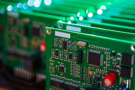
Whether designing a cell phone, tablet, portable computer, or other form of electronic product, good PCB layout in addition to PCB level shielding is essential to minimize EMI. Ground and power planes can be used as EMI shields for high threat noise signals, and this technique is a good first step towards minimizing the noise in these high threat signals. One problem with this approach is that RF energy will still radiate out of the component leads and package, so a more complete solution is needed. This is where PCB level shielding (also known as a “shielding can”) can be used to attenuate the noise emitted by these noisy devices.
To provide the greatest benefit, PCB level shielding must form a complete six-sided metal enclosure. This is achieved by soldering the shielding layer to a solid ground plane located below all components that need to be shielded. To maximize efficacy, there must not be any substantial gaps or openings in the ground plane. The actual performance of all shields and ground planes will always be affected by openings such as adjustment holes, indicators, wires, construction seams, and gaps between shielding can ground plane connections, so these items need to be avoided as much as possible.
The goal of EMI shielding is to create a Faraday cage around the enclosed RF noise components using the six sides of the metal box. The top five sides are made using a shielding cover or metal can, while the bottom sides are achieved using a ground plane within the PCB. In an ideal enclosure, no emissions would enter or leave the box. Unwanted emissions from these shields do occur, such as from holes punched into the tin can that allow heat transfer during solder reflow. These leaks can also be caused by defects in EMI gaskets or solder attachments. Noise can also escape from the spaces between the ground vias used to electrically connect the shield cover to the ground plane.
Traditionally, PCB shields are attached to the PCB using through-hole solder tails that are manually soldered after the main assembly process. This is a time-consuming and expensive process. If maintenance is required during installation and repair, desoldering is necessary to access the circuits and components under the shield. In densely populated areas of the PCB containing highly sensitive components, there is a high risk of expensive damage.
Typical properties of PCB level shielding cans are as follows:
Small footprint;
Low-profile configuration;
Two-piece design (fence and lid);
Through-hole or surface-mount;
Multiple-cavity pattern (isolate multiple components using the same shield);
Almost unlimited design flexibility;
Ventilation holes;
Removable lid for quick access to components;
I/O holes
Connector cutouts;
RF absorbers for enhanced shielding;
ESD protection with insulating pads;
Reliable protection against shock and vibration using a secure locking feature between frame and lid.
Typical shielding materials
A wide variety of shielding materials are commonly used, including brass, nickel silver, and stainless steel. The most common types are:
Small footprint;
Low-profile configuration;
Two-piece design (fence and cover);
Through-hole or surface mount;
Multiple cavity patterns (isolate multiple components using the same shield);
Almost unlimited design flexibility;
Ventilation holes;
Removable cover for quick access to components;
I/O holes
Connector cutouts;
RF absorbers for enhanced shielding;
ESD protection with insulating pads;
Reliable protection against shock and vibration using a secure locking feature between frame and cover.
Tin-plated steel is generally the best choice for shielding below 100 MHz, while tin-plated copper is the best choice for shielding above 200 MHz. Tin plating allows for the best soldering efficiency. Aluminum is not typically used for PCB level shielding because it does not have inherent heat dissipation properties and is not easily soldered to the ground plane.
Depending on the regulatory burden of the end product, all materials used for shielding may need to be RoHs compliant. In addition, if the product is used in hot and humid environments, it may cause galvanic corrosion and oxidation.

.png)