How to Use Return Paths for Better PCB Design
Introduction
Printed Circuit Board (PCB) design is a complex process that requires careful consideration of signal integrity, power distribution, and electromagnetic compatibility (EMC). One of the most critical yet often overlooked aspects of PCB design is the management of return paths for high-speed signals. A well-designed return path ensures minimal signal distortion, reduced electromagnetic interference (EMI), and improved overall performance.
This article explores the importance of return paths in PCB design, discusses different types of return paths, and provides practical guidelines for optimizing them to achieve better signal integrity and EMC compliance.
Understanding Return Paths
What is a Return Path?
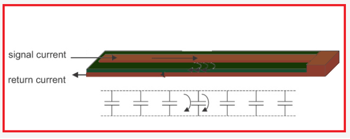
In a PCB, when a signal travels from a driver to a receiver, it forms a closed loop. The current flows through the signal trace and returns via a reference plane (usually ground or power). This return current path is essential for completing the circuit and maintaining signal integrity.
At high frequencies, return currents tend to follow the path of least impedance, which is directly beneath the signal trace on the reference plane. If the return path is disrupted (e.g., due to splits or gaps in the reference plane), the signal encounters impedance discontinuities, leading to reflections, crosstalk, and increased EMI.
Why is the Return Path Important?
- Signal Integrity – A continuous return path minimizes loop inductance, reducing signal distortion and ringing.
- EMI Reduction – A well-defined return path prevents high-frequency currents from radiating as noise.
- Impedance Control – Controlled impedance transmission lines (e.g., microstrips, striplines) rely on a solid reference plane for consistent performance.

Types of Return Paths
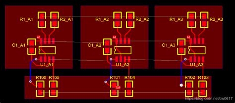
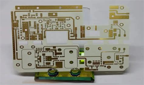
1. Ground Plane Return Path
Most PCBs use a solid ground plane as the primary return path. The return current flows directly beneath the signal trace, minimizing loop area and inductance.
Best Practices:
- Avoid splitting the ground plane under high-speed signals.
- Use multiple vias to connect ground layers in multilayer PCBs.
- Ensure ground stitching vias are placed near signal transitions (e.g., layer changes).
2. Power Plane Return Path
In some cases, high-speed signals reference a power plane instead of ground. This is common in mixed-signal designs where analog and digital grounds are separated.
Best Practices:
- Use decoupling capacitors to provide a low-impedance AC return path.
- Avoid routing high-speed signals over power plane splits.
- Ensure proper power distribution network (PDN) design to minimize noise.
3. Differential Pair Return Path
Differential signals (e.g., USB, PCIe) use a pair of traces where return currents cancel each other out, reducing EMI.
Best Practices:
- Maintain tight coupling between differential pairs.
- Ensure symmetrical routing to avoid common-mode noise.
- Avoid referencing different planes for the two traces in a pair.
Common Return Path Issues and Solutions
1. Split Planes and Gaps
If a signal crosses a split in the reference plane (e.g., a gap between ground and power), the return current is forced to take a longer path, increasing loop inductance and EMI.
Solution:
- Route high-speed signals away from plane splits.
- Use a “stitching capacitor” near the split to provide a high-frequency return path.
2. Layer Transitions
When a signal changes layers, the return current must find a new reference plane. If not properly managed, this can cause impedance mismatches.
Solution:
- Place ground vias adjacent to signal vias to ensure a continuous return path.
- Avoid referencing different planes (e.g., ground to power) without proper decoupling.
3. Discontinuous Ground Connections
In mixed-signal designs, improper grounding can lead to noise coupling between analog and digital sections.
Solution:
- Use a single-point ground or partitioned ground planes with controlled connections.
- Ensure high-speed digital signals do not cross analog ground regions.
Practical Guidelines for Optimizing Return Paths
1. Use a Solid Reference Plane
- Ensure uninterrupted ground/power planes beneath critical signal traces.
- Minimize cuts and slots in reference planes.
2. Control Signal Layer Stackup
- In multilayer PCBs, place high-speed signals adjacent to solid reference planes.
- Avoid referencing multiple planes for the same signal.
3. Proper Via Placement
- Use ground return vias near signal vias to maintain low inductance.
- Avoid long via stubs that can cause reflections.
4. Manage Differential Pairs Carefully
- Route differential pairs over the same reference plane.
- Maintain consistent spacing to avoid impedance variations.
5. Simulate and Validate
- Use field solvers and signal integrity tools (e.g., HyperLynx, ADS) to analyze return paths.
- Perform EMI testing to verify design effectiveness.
Conclusion
A well-designed return path is essential for high-speed PCB performance. By understanding how return currents flow and implementing best practices—such as maintaining continuous reference planes, optimizing layer stackups, and carefully managing layer transitions—designers can significantly improve signal integrity and reduce EMI.
As PCBs continue to operate at higher frequencies, attention to return paths will become even more critical. By applying the principles discussed in this article, engineers can achieve more reliable and efficient PCB designs.