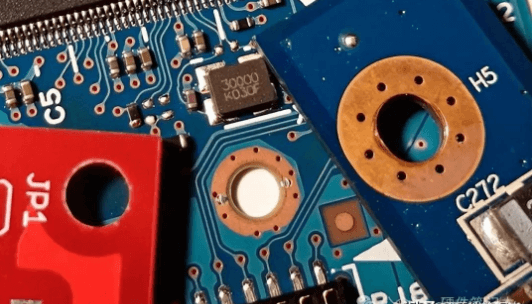
Multilayer board
Advantages Of Multilayer Boards In Modern Electronics
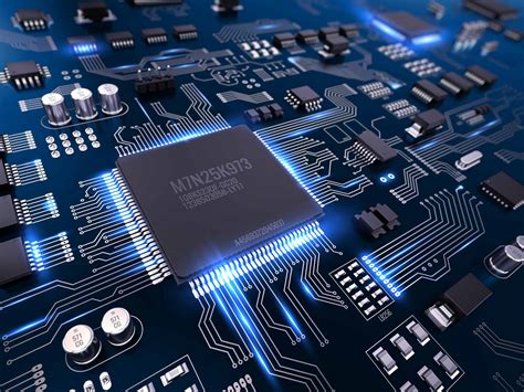
Multilayer boards have become a cornerstone in the realm of modern electronics, offering a multitude of advantages that cater to the ever-evolving demands of technology. As electronic devices continue to shrink in size while increasing in functionality, the need for more complex and efficient circuit boards has become paramount. Multilayer boards, which consist of multiple layers of conductive material separated by insulating layers, provide a solution that addresses these needs effectively.
One of the primary advantages of multilayer boards is their ability to support high-density circuits.
By stacking multiple layers, these boards can accommodate a greater number of components and connections within a limited space. This is particularly beneficial in the development of compact devices such as smartphones, tablets, and wearable technology, where space is at a premium. The increased density not only allows for more complex circuitry but also enhances the overall performance of the device by reducing the distance that electrical signals must travel.
In addition to supporting high-density circuits, multilayer boards offer improved electrical performance.
The close proximity of the layers allows for shorter signal paths, which in turn reduces signal loss and electromagnetic interference. This is crucial in high-speed applications where signal integrity is of utmost importance. Furthermore, the ability to incorporate ground and power planes within the board enhances its ability to manage power distribution and minimize noise, leading to more reliable and efficient electronic systems.
Another significant advantage of multilayer boards is their versatility in design.
Engineers have the flexibility to design intricate circuits that can meet specific requirements, thanks to the multiple layers available for routing. This flexibility is essential in the development of custom electronic solutions tailored to unique applications. Moreover, the use of computer-aided design (CAD) software in the design process allows for precise and efficient layout planning, ensuring optimal performance and manufacturability.
The durability and reliability of multilayer boards also contribute to their widespread adoption in modern electronics.
The layered construction provides structural integrity, making these boards more resistant to environmental stresses such as vibration and thermal expansion. This robustness is particularly important in applications where reliability is critical, such as in aerospace, automotive, and medical devices. The ability to withstand harsh conditions without compromising performance ensures that multilayer boards can be used in a wide range of demanding environments.
Furthermore, multilayer boards facilitate the integration of advanced technologies, such as surface mount technology (SMT) and through-hole technology (THT), which are essential for modern electronic manufacturing.
The compatibility with these technologies allows for efficient assembly processes and contributes to the miniaturization of electronic components. This integration capability not only streamlines production but also reduces costs, making multilayer boards an economically viable option for manufacturers.
In conclusion, the advantages of multilayer boards in modern electronics are manifold. Their ability to support high-density circuits, improve electrical performance, offer design versatility, and provide durability makes them an indispensable component in the development of cutting-edge electronic devices. As technology continues to advance, the role of multilayer boards in enabling innovation and enhancing device performance will undoubtedly remain significant. Their contribution to the miniaturization and efficiency of electronic systems underscores their importance in the ever-evolving landscape of modern electronics.
Design Considerations For Multilayer Printed Circuit Boards
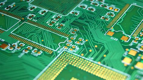
When designing multilayer printed circuit boards (PCBs), several critical considerations must be taken into account to ensure optimal performance and reliability. Multilayer PCBs, which consist of multiple layers of conductive material separated by insulating layers, are essential in modern electronics due to their ability to support complex circuitry in a compact form. As technology advances, the demand for smaller, more efficient devices continues to grow, making the design of multilayer PCBs increasingly important.
One of the primary considerations in multilayer PCB design is the selection of materials.
The choice of substrate material can significantly impact the board’s performance, particularly in terms of thermal management and signal integrity. Common materials include FR-4, a glass-reinforced epoxy laminate, which is widely used due to its balance of cost and performance. However, for high-frequency applications, materials with lower dielectric constants and loss tangents, such as PTFE-based laminates, may be more appropriate. The selection of materials must align with the specific requirements of the application, taking into account factors such as operating temperature, mechanical strength, and electrical performance.
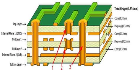
Another crucial aspect of multilayer PCB design is layer stack-up configuration.
The arrangement of layers within the PCB can affect signal integrity, electromagnetic compatibility, and thermal performance. A well-planned stack-up can minimize crosstalk and electromagnetic interference (EMI) while ensuring efficient heat dissipation. Typically, power and ground planes are strategically placed to provide a low-impedance path for return currents, which helps in reducing noise and improving signal quality. Additionally, the use of differential pairs and controlled impedance traces can further enhance signal integrity, especially in high-speed applications.
Transitioning to the topic of routing, the complexity of multilayer PCBs necessitates careful planning of trace routing to avoid issues such as signal degradation and impedance mismatches.
Designers must consider the width and spacing of traces, as well as the use of vias, which are conductive pathways that connect different layers of the PCB. While vias are essential for interlayer connectivity, excessive use can introduce parasitic inductance and capacitance, potentially affecting signal performance. Therefore, it is crucial to optimize via placement and minimize their number where possible.
Thermal management is another vital consideration in multilayer PCB design.
As electronic components become more powerful, they generate more heat, which can adversely affect performance and reliability if not properly managed. Effective thermal management strategies include the use of thermal vias, heat sinks, and thermal pads to dissipate heat away from critical components. Additionally, selecting materials with high thermal conductivity can aid in spreading heat more evenly across the board.
Finally, manufacturability and cost are important factors that must be balanced with performance requirements.
The complexity of multilayer PCBs can lead to increased manufacturing costs and longer production times. Therefore, designers should work closely with manufacturers to ensure that the design is not only functional but also economically viable. This collaboration can help identify potential issues early in the design process, reducing the likelihood of costly revisions later on.
In conclusion, the design of multilayer printed circuit boards involves a careful consideration of materials, layer stack-up, routing, thermal management, and manufacturability. By addressing these factors, designers can create PCBs that meet the demanding requirements of modern electronic devices, ensuring both performance and reliability. As technology continues to evolve, the importance of thoughtful multilayer PCB design will only grow, underscoring the need for expertise and innovation in this critical field.
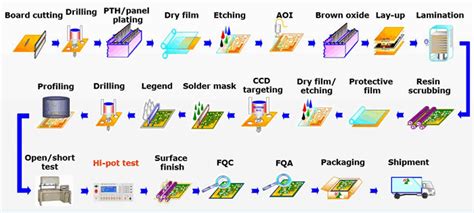
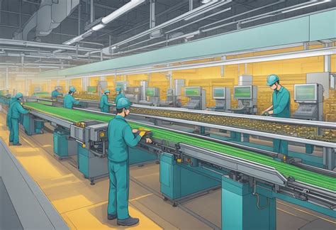
Manufacturing Process Of Multilayer PCBs: A Step-By-Step Guide
The manufacturing process of multilayer printed circuit boards (PCBs) is a complex and intricate procedure that requires precision and attention to detail. Multilayer PCBs are essential components in modern electronics, providing the necessary infrastructure for complex circuitry in compact spaces. The process begins with the design phase, where engineers use specialized software to create a detailed blueprint of the PCB. This design includes the layout of the circuits, the placement of components, and the routing of electrical connections. Once the design is finalized, it is converted into a format suitable for manufacturing.
The next step involves the preparation of the raw materials. Copper-clad laminates are the primary materials used in PCB manufacturing.
These laminates consist of a thin layer of copper foil bonded to a non-conductive substrate. The copper serves as the conductive layer, while the substrate provides structural support. The laminates are cleaned and prepared to ensure that they are free from any contaminants that could affect the quality of the final product.
Following the preparation of materials, the process of creating the inner layers begins.
This involves transferring the circuit design onto the copper-clad laminates using a technique called photolithography. A photosensitive film is applied to the copper surface, and the design is projected onto it using ultraviolet light. The exposed areas of the film harden, while the unexposed areas remain soft and are subsequently removed. This leaves a precise pattern of the circuit design on the copper surface.
Once the inner layers are created, they undergo an etching process to remove excess copper, leaving only the desired circuit pattern.
The etched layers are then inspected for defects and cleaned to remove any residual chemicals. After this, the layers are laminated together to form a single, cohesive board. This is achieved by stacking the layers in the correct order and applying heat and pressure to bond them together. The lamination process is critical, as it ensures the structural integrity and electrical performance of the multilayer PCB.
Drilling is the next step in the manufacturing process.
Holes are drilled into the laminated board to create vias, which are essential for establishing electrical connections between different layers. The precision of the drilling process is crucial, as any misalignment can lead to faulty connections and compromised functionality. After drilling, the holes are plated with copper to ensure conductivity.
The outer layers of the PCB are then created using a similar photolithography and etching process as the inner layers.
Once the outer layers are completed, the board undergoes a solder mask application. The solder mask is a protective layer that prevents solder bridges and short circuits during component assembly. It also provides a degree of protection against environmental factors such as moisture and dust.
Finally, the PCB is subjected to a series of tests to ensure its functionality and reliability. Electrical tests are conducted to verify that all connections are intact and that the board performs as intended. Any defects identified during testing are addressed before the board is approved for use. The manufacturing process of multilayer PCBs is a testament to the precision and expertise required to produce these vital components, which play a crucial role in the advancement of modern technology.
Comparing Single-Layer, Double-Layer, And Multilayer Boards: Which Is Right For Your Project?
When embarking on an electronic project, selecting the appropriate type of printed circuit board (PCB) is crucial to the success and functionality of the final product. The choice between single-layer, double-layer, and multilayer boards can significantly impact the design, cost, and performance of the device. Understanding the differences and advantages of each type can guide you in making an informed decision that aligns with your project’s requirements.
Single-layer boards, also known as single-sided PCBs, are the simplest form of circuit boards.
They consist of a single layer of conductive material, typically copper, on one side of a non-conductive substrate. These boards are ideal for low-density designs where the circuit complexity is minimal. Due to their straightforward design, single-layer boards are cost-effective and easy to manufacture, making them suitable for mass production. They are commonly used in consumer electronics, such as calculators and remote controls, where the demand for complex circuitry is limited. However, their simplicity also means they have limitations in terms of circuit density and functionality, which can be a drawback for more sophisticated applications.
Transitioning to double-layer boards, these offer a step up in complexity and capability.
Double-layer boards have conductive material on both sides of the substrate, allowing for more intricate circuit designs. This additional layer provides more space for routing connections, which can enhance the performance and functionality of the device. Double-layer boards are often used in applications that require moderate complexity, such as power supplies and industrial controls. They strike a balance between cost and capability, offering more flexibility than single-layer boards without the higher expense of multilayer options. However, they still have limitations in terms of the number of connections and the complexity of the circuits they can support.
For projects that demand high performance and intricate designs, multilayer boards are the optimal choice.
These boards consist of three or more layers of conductive material, separated by insulating layers, all laminated together. The multilayer design allows for a high density of connections and components, making them ideal for complex applications such as advanced computing systems, telecommunications equipment, and aerospace technology. The ability to incorporate multiple layers enables designers to create compact and efficient circuits that can handle high-speed signals and reduce electromagnetic interference. However, the complexity of multilayer boards comes with increased manufacturing costs and design challenges. The process of aligning and bonding multiple layers requires precision and expertise, which can extend production time and cost.
In conclusion, the decision between single-layer, double-layer, and multilayer boards should be guided by the specific needs and constraints of your project. Single-layer boards offer simplicity and cost-effectiveness for basic applications, while double-layer boards provide a middle ground with enhanced capabilities. Multilayer boards, though more expensive and complex, deliver superior performance for demanding applications. By carefully considering the requirements of your project, including factors such as circuit complexity, budget, and performance expectations, you can select the most appropriate type of PCB to ensure the success and efficiency of your electronic design.