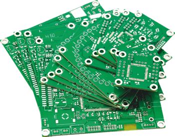
Multilayer pcb structure
Understanding The Basics Of Multilayer PCB Structure
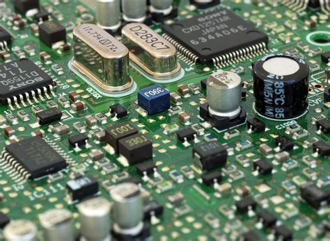
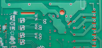
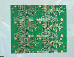
Multilayer printed circuit boards (PCBs) have become a cornerstone in modern electronics, providing the necessary infrastructure for complex and high-performance devices.
Understanding the basics of multilayer PCB structure is essential for anyone involved in electronics design and manufacturing.
At its core, a multilayer PCB consists of multiple layers of conductive material, typically copper, separated by insulating layers known as dielectric materials. These layers are laminated together under high pressure and temperature to form a single, cohesive unit.
The primary advantage of multilayer PCBs over their single-layer counterparts is their ability to support more complex and compact designs. By stacking multiple layers, designers can create intricate circuits that would be impossible to achieve on a single-layer board.
capability is particularly crucial in applications where space is at a premium, such as in smartphones, laptops, and medical devices. Moreover, multilayer PCBs can improve electrical performance by reducing the length of signal paths, thereby minimizing signal loss and electromagnetic interference.
Transitioning to the construction of multilayer PCBs, it begins with the inner layers, which are fabricated first.
These inner layers are etched to create the desired circuit patterns. Once the inner layers are prepared, they are laminated together with the outer layers using a process called lamination. During lamination, the layers are aligned precisely and bonded under heat and pressure. This process ensures that the layers are securely attached and that the board maintains its structural integrity.
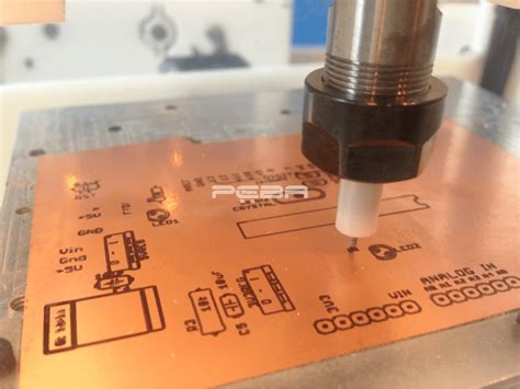
Following lamination, the next step is drilling.
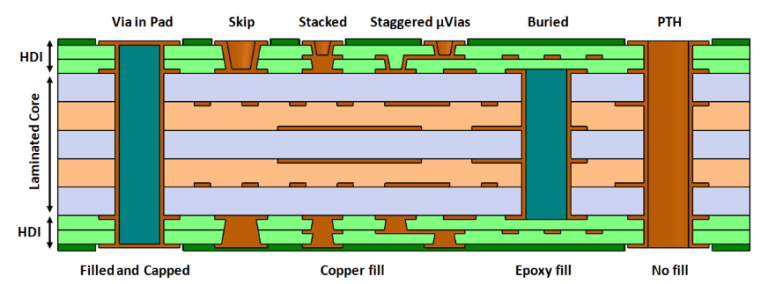
Holes, known as vias, are drilled through the board to create electrical connections between the different layers. These vias can be through-hole vias, which pass through the entire board, or blind/buried vias, which connect only specific layers. The choice of via type depends on the design requirements and the complexity of the circuit.
After drilling, the board undergoes a plating process to coat the walls of the vias with a conductive material, typically copper.
This step is crucial for establishing reliable electrical connections between the layers. Once the vias are plated, the outer layers are etched to create the final circuit patterns. This etching process is similar to that used for the inner layers and involves removing unwanted copper to leave behind the desired circuit traces.
To ensure the board’s functionality and reliability, it undergoes several testing and inspection stages.
Electrical testing verifies that the circuits are correctly connected and that there are no shorts or open circuits. Additionally, visual inspections and automated optical inspections (AOI) are performed to check for any physical defects, such as misaligned layers or incomplete etching.
In conclusion, the structure of a multilayer PCB is a complex yet meticulously organized assembly of conductive and insulating layers. This structure allows for the creation of highly sophisticated electronic devices that are both compact and efficient. By understanding the basics of multilayer PCB construction, one gains insight into the intricate processes that enable modern electronics to function seamlessly. As technology continues to advance, the demand for multilayer PCBs will only grow, underscoring their critical role in the future of electronic design and manufacturing.
Advantages Of Using Multilayer PCBs In Modern Electronics
Multilayer printed circuit boards (PCBs) have become a cornerstone in the development of modern electronics, offering a range of advantages that make them indispensable in various applications. One of the primary benefits of using multilayer PCBs is their ability to support complex circuitry within a compact form factor. As electronic devices continue to shrink in size while increasing in functionality, the demand for more intricate and densely packed circuits has grown. Multilayer PCBs address this need by allowing multiple layers of circuitry to be stacked upon one another, thereby maximizing the use of available space.
In addition to space efficiency, multilayer PCBs offer enhanced electrical performance.
The close proximity of the layers reduces the length of the electrical paths, which in turn minimizes signal loss and electromagnetic interference (EMI). This is particularly crucial in high-frequency applications where signal integrity is paramount. Furthermore, the ability to incorporate ground and power planes within the layers helps to stabilize the voltage levels and reduce noise, contributing to the overall reliability and performance of the electronic device.
Another significant advantage of multilayer PCBs is their design flexibility.
Engineers can create more complex and sophisticated designs by utilizing multiple layers, which allows for the integration of various components and functionalities within a single board. This flexibility is essential in the development of advanced technologies such as smartphones, medical devices, and aerospace systems, where precision and reliability are critical. The ability to design intricate circuits also enables the development of innovative products that push the boundaries of what is technologically possible.
Moreover, multilayer PCBs contribute to the durability and longevity of electronic devices.
The use of multiple layers provides additional mechanical strength, making the boards more resistant to bending and environmental stress. This is particularly important in applications where the devices are subjected to harsh conditions, such as in automotive or industrial settings. The robustness of multilayer PCBs ensures that the devices can withstand the rigors of daily use without compromising their performance.
Cost-effectiveness is another notable advantage of multilayer PCBs.
While the initial design and manufacturing process may be more complex and expensive compared to single-layer or double-layer PCBs, the long-term benefits often outweigh the initial costs. The ability to integrate multiple functions into a single board reduces the need for additional components and interconnections, which can lead to cost savings in the assembly and production stages. Additionally, the improved performance and reliability of multilayer PCBs can result in lower maintenance and replacement costs over the lifespan of the device.
Furthermore, the use of multilayer PCBs aligns with the growing trend towards miniaturization and increased functionality in electronic devices.
As consumer demand for smaller, more powerful gadgets continues to rise, manufacturers are increasingly turning to multilayer PCBs to meet these expectations. The ability to pack more functionality into a smaller footprint not only enhances the user experience but also opens up new possibilities for innovation and development in the electronics industry.
In conclusion, the advantages of using multilayer PCBs in modern electronics are manifold. From space efficiency and enhanced electrical performance to design flexibility, durability, and cost-effectiveness, multilayer PCBs offer a comprehensive solution to the challenges faced by today’s electronic designers and manufacturers. As technology continues to evolve, the role of multilayer PCBs in shaping the future of electronics is set to become even more significant, driving advancements and enabling the creation of cutting-edge devices that redefine what is possible.
Design Considerations For Multilayer PCB Fabrication
When embarking on the fabrication of multilayer printed circuit boards (PCBs), several design considerations must be meticulously evaluated to ensure optimal performance and reliability. The complexity inherent in multilayer PCBs necessitates a comprehensive understanding of various factors, including layer stack-up, material selection, signal integrity, thermal management, and manufacturing tolerances. Each of these elements plays a crucial role in the overall functionality and durability of the final product.
To begin with, the layer stack-up configuration is a fundamental aspect of multilayer PCB design.
The stack-up refers to the arrangement of conductive and insulating layers within the PCB. A well-planned stack-up can significantly enhance the electrical performance by minimizing electromagnetic interference (EMI) and crosstalk between signals. Typically, a multilayer PCB consists of alternating layers of copper and dielectric materials. The number of layers is determined by the complexity of the circuit and the need for additional routing space. For instance, high-speed digital circuits often require more layers to accommodate power and ground planes, which help in reducing noise and maintaining signal integrity.
Material selection is another critical consideration in multilayer PCB fabrication.
The choice of materials impacts not only the electrical properties but also the thermal and mechanical characteristics of the PCB. Commonly used dielectric materials include FR-4, polyimide, and Rogers laminates, each offering distinct advantages. FR-4, a glass-reinforced epoxy laminate, is widely used due to its cost-effectiveness and good electrical insulation properties. Polyimide, on the other hand, provides superior thermal stability, making it suitable for high-temperature applications. Rogers laminates are preferred for high-frequency applications due to their low dielectric constant and low loss tangent.
Signal integrity is paramount in multilayer PCB design, particularly for high-speed and high-frequency circuits.
Ensuring signal integrity involves careful consideration of trace impedance, trace width, and spacing. Controlled impedance traces are essential to prevent signal reflections and maintain signal quality. Additionally, differential pairs should be routed with consistent spacing to avoid skew and maintain signal synchronization. The use of ground planes and proper decoupling techniques further aids in mitigating noise and ensuring stable power delivery.
Thermal management is another vital aspect that cannot be overlooked.
As electronic components become more powerful and compact, effective heat dissipation becomes increasingly challenging. Multilayer PCBs can incorporate thermal vias, heat sinks, and thermal pads to facilitate efficient heat transfer away from critical components. Proper thermal management not only enhances the performance but also extends the lifespan of the PCB by preventing overheating and thermal stress.
Manufacturing tolerances and design for manufacturability (DFM) are also crucial considerations in multilayer PCB fabrication.
Tolerances in layer alignment, via placement, and trace width must be tightly controlled to ensure the PCB meets the required specifications. DFM principles should be applied to simplify the manufacturing process, reduce costs, and improve yield. This includes designing with standard panel sizes, minimizing the use of non-standard materials, and ensuring that the design can be easily tested and assembled.
In conclusion, the design considerations for multilayer PCB fabrication are multifaceted and interdependent. A thorough understanding of layer stack-up, material selection, signal integrity, thermal management, and manufacturing tolerances is essential to create a reliable and high-performance PCB. By meticulously addressing these factors, designers can achieve a balance between functionality, manufacturability, and cost-effectiveness, ultimately leading to the successful realization of complex electronic systems.
Common Challenges In Multilayer PCB Manufacturing And Solutions
Multilayer printed circuit boards (PCBs) are integral to modern electronic devices, offering enhanced functionality and compact design. However, the manufacturing process of multilayer PCBs presents several challenges that can impact the performance and reliability of the final product. Understanding these challenges and implementing effective solutions is crucial for manufacturers aiming to produce high-quality multilayer PCBs.
One of the primary challenges in multilayer PCB manufacturing is ensuring precise layer alignment.
Misalignment can lead to short circuits, open circuits, and other defects that compromise the board’s functionality. To address this issue, manufacturers employ advanced registration systems that use optical alignment techniques. These systems ensure that each layer is accurately positioned relative to the others, minimizing the risk of misalignment and improving overall yield.
Another significant challenge is managing the thermal expansion and contraction of different materials used in the PCB. Multilayer PCBs often consist of various materials with different coefficients of thermal expansion (CTE). During the manufacturing process, these materials can expand and contract at different rates, leading to warping, delamination, and other structural issues. To mitigate this problem, manufacturers carefully select materials with compatible CTEs and use controlled heating and cooling processes to minimize thermal stress.
The complexity of multilayer PCBs also introduces difficulties in achieving reliable interlayer connections.
Vias, which are small holes drilled through the layers to create electrical connections, must be precisely formed and plated to ensure proper conductivity. Any defects in the via formation or plating process can result in poor electrical performance or complete failure of the PCB. Advanced drilling techniques, such as laser drilling, and high-quality plating processes are employed to create robust and reliable vias.
Controlling the impedance of signal traces is another critical aspect of multilayer PCB manufacturing.
Impedance mismatches can lead to signal reflection, distortion, and loss, affecting the performance of high-speed circuits. Manufacturers use precise design and simulation tools to calculate the optimal trace widths, spacing, and layer stack-up to achieve the desired impedance. Additionally, controlled impedance testing is performed during production to verify that the manufactured PCBs meet the specified impedance requirements.
The increasing demand for miniaturization and higher component density in electronic devices further complicates multilayer PCB manufacturing.
As the size of components and traces decreases, maintaining the integrity of the PCB becomes more challenging. Fine-line etching techniques and advanced photolithography processes are employed to create narrow traces and small features with high precision. Moreover, manufacturers use advanced inspection and testing methods, such as automated optical inspection (AOI) and X-ray inspection, to detect and rectify any defects that may arise during the manufacturing process.
Finally, ensuring the reliability and durability of multilayer PCBs in harsh operating environments is a significant concern.
Factors such as temperature fluctuations, humidity, and mechanical stress can degrade the performance of the PCB over time. To enhance reliability, manufacturers use high-quality materials, such as high-temperature laminates and advanced solder masks, that can withstand extreme conditions. Additionally, rigorous testing, including thermal cycling, humidity testing, and mechanical stress testing, is conducted to validate the durability of the PCBs.
In conclusion, while multilayer PCB manufacturing presents several challenges, advancements in technology and manufacturing processes have enabled manufacturers to overcome these obstacles effectively. By employing precise alignment techniques, managing thermal expansion, ensuring reliable interlayer connections, controlling impedance, and addressing miniaturization challenges, manufacturers can produce high-quality multilayer PCBs that meet the demands of modern electronic devices. Furthermore, rigorous testing and the use of high-quality materials ensure the reliability and durability of these PCBs in various operating environments.