Optimizing PCB Fabrication and Assembly for Superior Performance

Key Takeaways
Effective PCB fabrication and pcb assembly processes rely on precision-driven methodologies to ensure optimal performance in electronic systems. Key considerations include design validation, material selection, and thermal management, which collectively influence the reliability of PCBA (Printed Circuit Board Assembly).
Tip: Always conduct a Design for Manufacturability (DFM) review early in the process to identify potential bottlenecks in pcb assembly workflows.
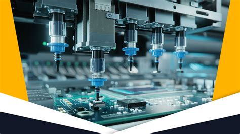
Integrating automated optical inspection (AOI) during pcb assembly minimizes defects, while advanced soldering techniques like reflow or wave soldering enhance connection integrity. For fabrication, leveraging laser drilling and controlled impedance routing ensures high-density interconnects meet signal integrity requirements. Additionally, selecting high-Tg materials and low-loss laminates can significantly improve thermal and electrical performance in PCBA applications.
Transitioning between fabrication and assembly stages demands strict adherence to industry standards (e.g., IPC-A-610), ensuring compatibility across processes. By prioritizing quality-driven testing—such as in-circuit testing (ICT) and functional testing—manufacturers can preemptively address failures, reducing rework costs. These strategies, when harmonized, create a robust framework for achieving superior reliability in complex electronic systems.

Essential Techniques for Reliable PCB Manufacturing
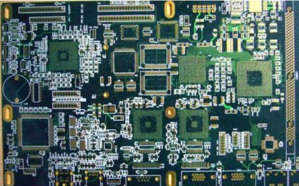
Achieving consistent reliability in PCB fabrication demands adherence to precision-driven processes and rigorous quality protocols. Central to this is optimizing material selection, where substrates like FR4 or high-frequency laminates are chosen based on thermal stability and signal integrity requirements. Equally critical is ensuring trace width consistency and via integrity during etching, as deviations can compromise electrical performance.
In PCB assembly (PCBA), solder paste application accuracy directly impacts joint reliability. Employing automated stencil printing minimizes voids, while reflow profiling ensures proper alloy bonding. For mixed-technology boards, combining surface-mount (SMT) and through-hole components requires precise thermal management to prevent warping or delamination.
Advanced inspection methods, such as automated optical inspection (AOI) and X-ray imaging, validate alignment and solder quality post-assembly. Additionally, implementing environmental stress testing—including thermal cycling and vibration simulations—identifies potential failure points before deployment. By integrating these techniques, manufacturers mitigate risks in PCBA workflows, ensuring boards meet stringent performance benchmarks across industries like aerospace and medical electronics.

Key Factors in High-Performance PCB Assembly
Achieving high-performance PCB assembly hinges on balancing technical precision with rigorous quality control. The foundation begins with material selection, where thermal stability and signal integrity dictate choices in substrate laminates and conductive layers. Advanced pcb assembly workflows integrate automated pick-and-place systems to ensure micron-level accuracy for surface-mount devices (SMDs), minimizing placement errors that compromise electrical performance.
PCBA reliability further depends on solder joint integrity, requiring precise reflow profiling to prevent voids or cold joints. Implementing automated optical inspection (AOI) and X-ray testing at critical stages identifies latent defects, such as micro-cracks or misaligned components, before final integration. Environmental stressors like humidity and thermal cycling are mitigated through conformal coatings, which enhance durability in harsh operating conditions.
Equally critical is design-for-manufacturability (DFM) collaboration between engineers and pcb assembly teams. Proactive DFM reviews address potential bottlenecks, such as inadequate pad spacing or via placement, streamlining production while adhering to IPC-A-610 standards. By prioritizing these factors, manufacturers elevate PCBA outcomes, delivering boards that meet high-frequency, high-power, and miniaturization demands without sacrificing reliability.
Advanced Methods to Enhance PCB Fabrication Quality
Achieving superior PCB fabrication quality requires integrating cutting-edge techniques with rigorous process controls. Modern manufacturers employ automated optical inspection (AOI) systems to detect microscopic defects in copper traces or solder masks, reducing human error by over 40%. For high-density designs, laser direct imaging (LDI) ensures precise alignment of circuit patterns, critical for minimizing signal loss in high-frequency applications.
Material selection plays a pivotal role: using low-CTE (coefficient of thermal expansion) substrates enhances thermal stability, while advanced surface finishes like ENIG (Electroless Nickel Immersion Gold) improve solderability and corrosion resistance. To address warping risks, optimized lamination protocols balance temperature and pressure during multilayer bonding.
| Parameter | Traditional Method | Advanced Optimization |
|---|---|---|
| Trace Width Tolerance | ±15% | ±5% (via LDI) |
| Via Reliability | 85% at 1000 cycles | 98% (with filled vias) |
| Thermal Stress Resistance | 260°C for 10s | 300°C for 30s (halogen-free) |
In PCBA workflows, combining design for manufacturability (DFM) checks with real-time process monitoring ensures seamless transitions from fabrication to assembly. For instance, impedance-controlled routing paired with 3D solder paste inspection (SPI) reduces rework rates by 25% in complex pcb assembly projects. By adopting these methodologies, manufacturers systematically elevate yield rates while meeting stringent performance benchmarks for mission-critical electronics.
Best Practices for Precision PCB Engineering
Achieving excellence in PCB fabrication and assembly begins with rigorous attention to design accuracy and material selection. Engineers must prioritize design for manufacturability (DFM) principles, ensuring layouts account for thermal management, signal integrity, and mechanical stability. For instance, optimizing trace widths and spacing minimizes impedance mismatches, while selecting high-grade substrates like FR-4 or polyimide enhances durability in demanding environments.
During PCBA (printed circuit board assembly), precise solder paste application and component placement are critical. Automated pick-and-place systems paired with 3D solder paste inspection (SPI) reduce defects such as bridging or misalignment. Additionally, adhering to IPC-A-610 standards for cleanliness and soldering quality ensures long-term reliability. Thermal profiling during reflow soldering further prevents stress-induced failures, particularly in multi-layer boards.
Collaboration between design and manufacturing teams streamlines PCB assembly workflows, enabling rapid prototyping and iterative testing. Advanced simulation tools, such as finite element analysis (FEA), predict thermal and mechanical behavior, allowing preemptive adjustments. By integrating these strategies, manufacturers achieve first-pass yield optimization while maintaining compliance with industry benchmarks for PCBA performance. This systematic approach not only reduces costs but also accelerates time-to-market for high-performance electronic systems.
Critical Steps in Optimizing Assembly Processes
Achieving peak performance in PCB assembly requires a precision-driven approach to process refinement. Central to this is implementing automated optical inspection (AOI) systems to detect solder joint defects or misaligned components during PCBA stages. Optimizing solder paste application through stencil design improvements and temperature-controlled reflow profiles ensures consistent electrical connectivity, while rigorous component placement accuracy minimizes signal interference risks.
Equally vital is adopting design for manufacturability (DFM) principles early in the PCB fabrication phase, which reduces assembly complexities and material waste. Integrating traceability systems for critical components, such as BGAs or microcontrollers, enhances quality control across high-volume production. Advanced techniques like X-ray inspection further validate hidden connections in multilayer boards, addressing reliability concerns in compact designs.
Furthermore, balancing thermal management strategies—such as selecting thermally conductive substrates or optimizing via placement—prevents overheating during operation. Pairing these steps with real-time process monitoring tools creates closed-loop feedback, enabling rapid adjustments to assembly parameters. By aligning PCBA workflows with industry-certified standards like IPC-A-610, manufacturers ensure compliance while delivering boards that meet stringent performance benchmarks. This systematic optimization fosters repeatable outcomes, positioning PCB assembly as a cornerstone of dependable electronic systems.
Innovative Approaches to PCB Reliability Improvement
Advancements in PCB assembly techniques are reshaping how manufacturers address reliability challenges in modern electronics. By integrating material science innovations with precision-driven PCBA workflows, engineers can mitigate common failure modes such as thermal stress and signal degradation. One emerging strategy involves the use of low-loss dielectric materials in substrate fabrication, which reduces impedance variations and enhances signal integrity across high-frequency circuits. Additionally, implementing embedded component technology during PCB assembly minimizes solder joint vulnerabilities, a critical factor in applications exposed to mechanical shock or vibration.
To further bolster reliability, progressive manufacturers are adopting predictive analytics to monitor PCBA processes in real time. Machine learning algorithms analyze historical production data to identify patterns that correlate with field failures, enabling preemptive adjustments in lamination parameters or solder paste application. Pairing this with automated optical inspection (AOI) systems ensures microscopic defects—such as micro-cracks or insufficient via fills—are detected before final integration. For mission-critical systems, conformal coating advancements provide robust environmental protection without compromising heat dissipation, addressing the dual demands of durability and thermal management.
These methodologies, when combined with rigorous design-for-reliability (DFR) principles, create a synergistic framework for elevating PCB assembly outcomes. By prioritizing both process innovation and material optimization, manufacturers can deliver PCBA solutions that meet the escalating performance demands of aerospace, automotive, and IoT applications.

Proven Strategies for Quality-Driven PCB Production
Implementing quality-driven methodologies in PCB assembly requires a systematic approach that integrates design validation, process controls, and rigorous testing. Central to this strategy is adopting Design for Manufacturability (DFM) principles, which minimize errors during PCBA by aligning design specifications with production capabilities. Advanced manufacturers employ real-time monitoring of solder paste application and component placement to ensure micron-level precision, reducing rework rates by up to 40%.
Emphasizing traceability across the PCB fabrication and assembly workflow enhances accountability, with serialized tracking of materials and process parameters. Pairing this with Automated Optical Inspection (AOI) and X-ray testing ensures defects are identified early, maintaining compliance with standards like IPC-A-610 and ISO 9001. For high-reliability applications, thermal cycling tests and environmental stress screening validate board durability under extreme conditions.
Collaboration between design engineers and PCBA specialists further optimizes outcomes, particularly in addressing signal integrity challenges and thermal management requirements. By prioritizing data-driven refinements and investing in certified PCB assembly infrastructure, manufacturers consistently achieve >99.5% yield rates while scaling production efficiently. This holistic focus on quality assurance transforms PCB fabrication from a transactional process into a strategic advantage for electronic systems.
Conclusion
The pursuit of excellence in PCB fabrication and assembly demands a holistic approach that integrates precision engineering with rigorous quality control. By aligning pcb assembly workflows with advanced fabrication methodologies, manufacturers can achieve uncompromised reliability in electronic systems. Critical steps such as design validation, material compatibility analysis, and automated optical inspection (AOI) ensure that PCBA outputs meet stringent performance benchmarks. Furthermore, adopting data-driven process optimization minimizes defects while enhancing throughput, particularly in high-volume production environments.
To sustain competitive advantage, manufacturers must prioritize thermal management solutions and signal integrity testing during pcb assembly, as these factors directly influence long-term operational stability. Collaboration between fabrication and PCBA teams remains pivotal, enabling seamless transitions from prototyping to mass production. By embedding traceability mechanisms and real-time monitoring into workflows, stakeholders can swiftly address deviations, ensuring compliance with industry standards. Ultimately, the convergence of precision fabrication and intelligent assembly techniques establishes a foundation for innovation, driving the next generation of electronics toward peak performance and durability.
FAQs
What distinguishes PCB fabrication from PCB assembly?
PCB fabrication involves creating the bare board through processes like etching, layering, and drilling, while PCB assembly (PCBA) refers to populating the board with components like resistors, ICs, and connectors. Both stages require precision to ensure optimal functionality.
How do material choices impact PCB reliability?
Selecting high-grade substrates, copper thickness, and solder masks directly affects thermal management, signal integrity, and longevity. For PCBA, using certified components and lead-free solder reduces failure risks in harsh environments.
What quality checks are critical during PCBA?
Automated optical inspection (AOI), X-ray testing, and functional testing validate solder joint integrity, component alignment, and electrical performance. These steps prevent defects like shorts or open circuits in final products.
Can design-for-manufacturing (DFM) principles reduce assembly errors?
Yes. DFM guidelines, such as optimizing pad sizes and spacing, minimize soldering issues and improve yield. Collaborating with PCBA providers early in design ensures manufacturability without compromising performance.
Why is thermal management vital in high-density PCB assemblies?
Dense layouts generate excess heat, risking component degradation. Techniques like thermal vias, heatsinks, and proper layer stacking dissipate heat efficiently, ensuring stability in high-power applications.
Ready to Elevate Your PCB Projects?
For expert guidance on PCB assembly and fabrication tailored to your needs, please click here to explore AndwinPCB’s advanced solutions.