PCB Circuit Board Short Circuit Inspection and Prevention
Introduction
Printed Circuit Boards (PCBs) are the backbone of modern electronic devices, providing the necessary electrical connections between components. However, one of the most common and critical issues in PCB manufacturing and operation is short circuits. A short circuit occurs when an unintended low-resistance connection forms between two or more conductive paths, leading to excessive current flow, overheating, and potential device failure.
Detecting and preventing short circuits in PCBs is essential for ensuring reliability, safety, and longevity of electronic products. This article explores the causes of PCB short circuits, inspection methods, and preventive measures.
Causes of PCB Short Circuits
Understanding the root causes of short circuits helps in implementing effective prevention strategies. Common causes include:
1. Design Errors
- Insufficient Clearance: If traces or pads are too close, solder bridging or conductive debris can create a short.
- Improper Via Placement: Vias placed too close to other conductive elements may lead to unintended connections.
- Incorrect Net Assignments: Errors in schematic design can cause unintended connections between nets.
2. Manufacturing Defects
- Solder Bridging: Excess solder between adjacent pins or traces can create a short.
- Copper Residuals: Improper etching can leave conductive copper remnants, forming unintended paths.
- Drilling Misalignment: Holes or vias drilled in the wrong location can connect unrelated layers.
3. Component Issues
- Faulty Components: Damaged or defective components may internally short.
- Incorrect Placement: Misaligned or reversed components can cause shorts.
4. Environmental Factors
- Moisture and Contamination: Conductive dust, humidity, or liquid spills can create leakage paths.
- Mechanical Stress: Flexing or impact can damage traces, leading to shorts.
Methods for Inspecting PCB Short Circuits
Early detection of short circuits is crucial to avoid catastrophic failures. Several inspection techniques are available:
1. Visual Inspection
- Manual Examination: Using a magnifying glass or microscope to check for solder bridges, damaged traces, or misplaced components.
- Automated Optical Inspection (AOI): Cameras and software scan PCBs for defects like solder splashes or misalignments.
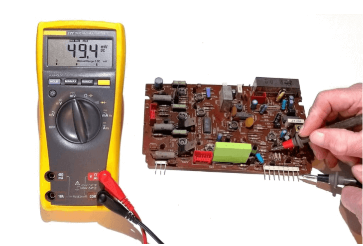
2. Continuity Testing (Multimeter Check)
- Resistance Measurement: A multimeter in continuity mode checks for unexpected low resistance between traces.
- Diode Mode Test: Helps detect shorts in power and ground planes.
3. Thermal Imaging
- Infrared cameras detect heat spots caused by excessive current flow due to shorts.
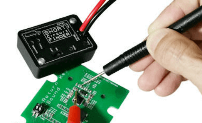
4. Flying Probe Testing
- Automated test probes check electrical connectivity and isolate shorted nets.
5. X-Ray Inspection
- Useful for detecting hidden shorts in multilayer PCBs, such as via misalignment or internal layer defects.
6. Current Tracing with a Power Supply
- Applying limited current and using a thermal camera to locate hotspots indicating a short.
Preventive Measures for PCB Short Circuits
Preventing short circuits requires attention during design, manufacturing, and assembly:
1. Design Best Practices
- Adequate Trace Spacing: Follow IPC standards for minimum clearance between traces.
- Proper Grounding Techniques: Use ground planes effectively to minimize noise and unintended paths.
- DFM (Design for Manufacturability) Checks: Ensure the design is optimized for fabrication and assembly.
2. Manufacturing Controls
- Controlled Soldering Process: Use solder masks and stencils to prevent bridging.
- Proper Etching: Ensure complete removal of unwanted copper.
- Automated Optical Inspection (AOI): Implement AOI to catch defects early.
3. Component and Assembly Precautions
- Correct Component Placement: Follow datasheet guidelines for orientation and spacing.
- Use of Conformal Coating: Protects against moisture and contamination.
- ESD Protection: Prevents electrostatic discharge damage that may cause latent shorts.
4. Testing and Quality Assurance
- In-Circuit Testing (ICT): Validates electrical performance before deployment.
- Burn-In Testing: Stress-tests PCBs to identify latent defects.
5. Handling and Storage
- Avoid Mechanical Stress: Prevent bending or dropping PCBs.
- Moisture Control: Store PCBs in dry environments or use desiccants.
Conclusion
Short circuits in PCBs can lead to device malfunctions, safety hazards, and costly repairs. By understanding the causes—such as design flaws, manufacturing errors, and environmental factors—engineers can implement effective inspection techniques like visual checks, multimeter testing, and thermal imaging.
Preventive strategies, including proper design practices, controlled manufacturing, and rigorous testing, are essential for minimizing short circuit risks. Implementing these measures ensures reliable, high-performance PCB assemblies, reducing failure rates and enhancing product longevity.
By adopting a proactive approach to PCB inspection and prevention, manufacturers and designers can significantly improve electronic product quality and reliability.