Pcb design process
Understanding The Basics Of PCB Design process
Printed Circuit Board (PCB) design is a critical aspect of modern electronics, serving as the foundation upon which electronic components are mounted and interconnected. Understanding the basics of PCB design is essential for anyone involved in electronics engineering, as it ensures the functionality, reliability, and manufacturability of electronic devices.
The process begins with a clear understanding of the requirements and constraints of the project, which includes defining the electrical, mechanical, and environmental specifications.
Initially, the design process involves creating a schematic diagram, which is a symbolic representation of the electronic circuit.
This diagram outlines the components and their connections, providing a blueprint for the subsequent stages of PCB design. The schematic is created using specialized software tools that allow designers to place components and draw connections between them. This step is crucial as it lays the groundwork for the physical layout of the PCB.
Once the schematic is complete, the next step is to translate it into a physical layout.
This involves placing the components on the PCB and routing the electrical connections between them. The placement of components is a critical task that requires careful consideration of various factors, such as signal integrity, thermal management, and manufacturability. Components must be placed in a manner that minimizes the length of critical signal paths and reduces electromagnetic interference. Additionally, thermal considerations are essential to ensure that heat-generating components are adequately spaced and that there is sufficient airflow for cooling.
Routing, the process of connecting the components with copper traces, is another vital aspect of PCB design.
Designers must ensure that the traces are of appropriate width and spacing to handle the required current and to prevent short circuits. High-speed signals require special attention to maintain signal integrity, often necessitating controlled impedance traces and differential pair routing. Furthermore, power and ground planes are typically included to provide stable voltage levels and to reduce noise.
Design rules and constraints play a significant role in guiding the layout and routing process.
These rules are defined based on the capabilities of the manufacturing process and the performance requirements of the circuit. Adhering to these rules ensures that the PCB can be reliably manufactured and that it will function as intended. Design rule checks (DRC) are performed throughout the design process to identify and rectify any violations.
After the layout and routing are complete, the design undergoes a series of verification steps.
Electrical rule checks (ERC) and signal integrity analysis are conducted to ensure that the circuit will perform correctly under various conditions. Additionally, thermal analysis may be performed to verify that the PCB can dissipate heat effectively. Once the design passes these verification steps, it is ready for fabrication.
The final stage of the PCB design process involves generating the necessary files for manufacturing.
These files, known as Gerber files, contain detailed information about the PCB’s layers, including copper traces, solder mask, and silkscreen. The Gerber files are sent to a PCB manufacturer, who fabricates the board according to the specifications.
In conclusion, understanding the basics of PCB design is fundamental for creating reliable and functional electronic devices. The process involves several critical steps, including schematic creation, component placement, routing, and verification. By adhering to design rules and performing thorough checks, designers can ensure that their PCBs meet the required specifications and can be successfully manufactured.
Key Steps In The PCB Design Process
The printed circuit board (PCB) design process is a critical aspect of modern electronics, serving as the foundation upon which electronic devices are built. This intricate process involves several key steps, each of which must be meticulously executed to ensure the final product meets the desired specifications and functions correctly. Understanding these steps is essential for anyone involved in electronics design and manufacturing.
The initial phase of the PCB design process begins with defining the requirements and specifications of the project.
This involves a thorough understanding of the device’s functionality, the components to be used, and the overall design constraints. Engineers and designers collaborate to create a detailed schematic diagram, which serves as a blueprint for the PCB. This schematic outlines the electrical connections between various components, ensuring that the circuit will function as intended.
Once the schematic is finalized, the next step is to select the appropriate components.
This involves choosing parts that meet the required specifications, such as resistors, capacitors, and integrated circuits. Component selection is a critical step, as it directly impacts the performance and reliability of the final product. Designers must consider factors such as component availability, cost, and compatibility with the overall design.
With the components selected, the focus shifts to the layout design.
This step involves arranging the components on the PCB in a manner that optimizes space and ensures efficient electrical connections. Designers use specialized software tools to create a virtual representation of the PCB, allowing them to experiment with different layouts and configurations. During this phase, it is crucial to consider factors such as signal integrity, thermal management, and electromagnetic compatibility.
Following the layout design, the next step is to create the routing of the PCB.
Routing involves connecting the various components using conductive traces, which are essentially pathways for electrical signals. This step requires careful planning to minimize signal interference and ensure reliable connections. Designers must also consider the physical constraints of the PCB, such as the number of layers and the available space for routing.
After the routing is complete, the design undergoes a series of checks and validations.
This includes design rule checks (DRC) to ensure that the layout adheres to manufacturing constraints and electrical rule checks (ERC) to verify the correctness of the electrical connections. These checks are essential to identify and rectify any potential issues before proceeding to the manufacturing stage.
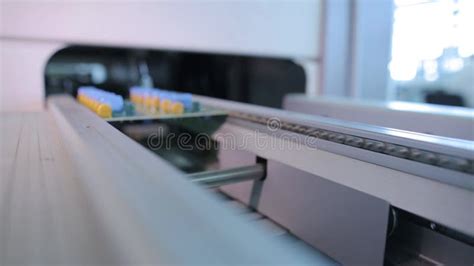
Once the design has passed all checks, the next step is to generate the necessary files for manufacturing.
These files, known as Gerber files, contain detailed information about the PCB layout, including the placement of components, routing of traces, and other critical details. The Gerber files are then sent to a PCB manufacturer, who uses them to fabricate the physical PCB.
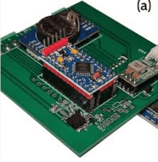
The final step in the PCB design process is assembly and testing.
During assembly, the selected components are soldered onto the fabricated PCB, creating a complete electronic circuit. This is followed by rigorous testing to ensure that the PCB functions as intended. Testing may involve functional tests, signal integrity tests, and environmental tests to verify the reliability and performance of the PCB under various conditions.
In conclusion, the PCB design process is a complex and multifaceted endeavor that requires careful planning, precise execution, and thorough validation. Each step, from defining requirements to assembly and testing, plays a crucial role in ensuring the success of the final product. By understanding and adhering to these key steps, designers can create reliable and high-performance PCBs that meet the demands of modern electronic devices.
Common Mistakes To Avoid In PCB Design
In the intricate world of PCB design, even the smallest mistake can lead to significant issues, ranging from minor performance inefficiencies to complete system failures. Understanding common pitfalls and how to avoid them is crucial for any designer aiming to produce reliable and efficient printed circuit boards.
One of the most frequent errors in PCB design is inadequate planning.
Designers often rush into the layout phase without thoroughly considering the overall design requirements, such as component placement, signal integrity, and thermal management. This lack of foresight can result in a cluttered and inefficient board that is difficult to troubleshoot and modify.
Another prevalent mistake is improper component placement.
Components should be strategically placed to minimize signal path lengths and reduce electromagnetic interference (EMI). Placing components haphazardly can lead to increased noise and signal degradation, which can severely impact the performance of the PCB. Additionally, failing to consider the physical size and orientation of components can lead to mechanical issues during assembly, such as misalignment or insufficient solder joint strength.
Transitioning to the topic of routing, improper trace width and spacing are common errors that can compromise the functionality of a PCB.
Traces that are too narrow may not be able to handle the required current, leading to overheating and potential failure. Conversely, traces that are too wide can take up unnecessary space and complicate the routing process. Similarly, inadequate spacing between traces can result in short circuits and signal crosstalk, which can degrade the performance of the board.
Grounding issues are another critical area where mistakes frequently occur.
A poorly designed ground plane can lead to ground loops, which can introduce noise and interfere with signal integrity. Ensuring a continuous and unbroken ground plane is essential for maintaining a stable reference voltage and minimizing EMI. Additionally, designers should avoid placing vias in the ground plane, as this can create discontinuities that disrupt the flow of current.
Thermal management is often overlooked, yet it is a vital aspect of PCB design.
Components that generate significant heat need to be adequately cooled to prevent overheating and ensure long-term reliability. Failing to incorporate sufficient thermal vias, heat sinks, or copper pours can lead to hot spots and thermal stress, which can degrade the performance and lifespan of the PCB. Proper thermal management involves not only addressing individual components but also considering the overall heat distribution across the board.
Another common mistake is neglecting to perform thorough design rule checks (DRCs) and electrical rule checks (ERCs).
These automated checks can identify potential issues such as trace width violations, clearance problems, and unconnected nets. Skipping these checks can result in undetected errors that may only become apparent during manufacturing or testing, leading to costly rework and delays.
Finally, communication with the manufacturing team is crucial to avoid misunderstandings and ensure that the design can be efficiently produced.
Providing clear and detailed documentation, including fabrication drawings, assembly instructions, and a bill of materials (BOM), can help prevent errors during the manufacturing process. Failing to communicate effectively with the manufacturer can result in production delays, increased costs, and suboptimal board performance.
In conclusion, avoiding common mistakes in PCB design requires careful planning, strategic component placement, proper routing, effective grounding, adequate thermal management, thorough rule checking, and clear communication with the manufacturing team. By paying attention to these critical areas, designers can create reliable and efficient PCBs that meet the desired performance specifications and stand the test of time.
Advanced Techniques For Optimizing PCB Layout
The process of designing printed circuit boards (PCBs) has evolved significantly over the years, with advanced techniques now available to optimize PCB layout for performance, reliability, and manufacturability. One of the primary considerations in advanced PCB layout is signal integrity, which involves ensuring that signals are transmitted without degradation. To achieve this, designers often employ techniques such as controlled impedance routing, differential pair routing, and proper termination. Controlled impedance routing ensures that the impedance of the traces matches the impedance of the components, thereby minimizing signal reflections and maintaining signal integrity.
In addition to signal integrity, thermal management is another critical aspect of advanced PCB layout.
As electronic components become more powerful and compact, they generate more heat, which can affect performance and reliability. Effective thermal management techniques include the use of thermal vias, heat sinks, and thermal pads. Thermal vias are small holes filled with conductive material that help dissipate heat from the surface of the PCB to the inner layers or to an external heat sink. Heat sinks and thermal pads provide additional pathways for heat to escape, ensuring that components remain within their safe operating temperatures.
Furthermore, power integrity is essential for the proper functioning of a PCB.
Power integrity involves ensuring that the power delivered to each component is stable and free from noise. Techniques such as proper decoupling capacitor placement, power plane segmentation, and the use of low-impedance power distribution networks are crucial. Decoupling capacitors help filter out noise and provide a stable power supply to the components. Power plane segmentation involves dividing the power plane into different sections to isolate noisy components from sensitive ones, thereby reducing the risk of interference.
Another advanced technique for optimizing PCB layout is the use of design for manufacturability (DFM) principles.
DFM involves designing the PCB in a way that makes it easier and more cost-effective to manufacture. This includes considerations such as component placement, trace width, and spacing, as well as the use of standard footprints and pad sizes. By adhering to DFM principles, designers can reduce the likelihood of manufacturing defects and improve the overall yield of the PCB production process.
Moreover, electromagnetic compatibility (EMC) is a crucial factor in advanced PCB layout.
EMC involves designing the PCB to minimize electromagnetic interference (EMI) and ensure that the board does not interfere with other electronic devices. Techniques such as proper grounding, shielding, and the use of ferrite beads can help achieve good EMC performance. Proper grounding involves creating a low-impedance path to ground for high-frequency signals, while shielding involves enclosing sensitive components in a conductive enclosure to block EMI. Ferrite beads are used to filter out high-frequency noise from power and signal lines.
Lastly, the use of advanced simulation and analysis tools is indispensable in modern PCB design.
These tools allow designers to model and analyze various aspects of the PCB, such as signal integrity, thermal performance, and power integrity, before the board is manufactured. By using simulation tools, designers can identify and address potential issues early in the design process, reducing the risk of costly rework and ensuring that the final product meets all performance and reliability requirements.
In conclusion, optimizing PCB layout involves a combination of advanced techniques that address signal integrity, thermal management, power integrity, manufacturability, and electromagnetic compatibility. By employing these techniques and leveraging advanced simulation tools, designers can create high-performance, reliable, and cost-effective PCBs that meet the demands of modern electronic applications.


