PCB Design Using Cadence Allegro: A Comprehensive Guide
Introduction
Printed Circuit Board (PCB) design is a critical aspect of modern electronics, enabling the development of complex circuits in compact and efficient layouts. Among the various PCB design tools available, Cadence Allegro stands out as one of the most powerful and widely used software solutions for professional PCB design. This article explores the key features, workflow, and advantages of using Cadence Allegro for PCB design, along with best practices for engineers and designers.
1. Overview of Cadence Allegro
Cadence Allegro is a high-performance PCB design and analysis tool developed by Cadence Design Systems, a leader in electronic design automation (EDA). Allegro provides a comprehensive environment for schematic capture, PCB layout, signal integrity analysis, and manufacturing preparation. It is widely used in industries such as aerospace, automotive, telecommunications, and consumer electronics due to its scalability, precision, and advanced features.
Key Features of Allegro
- Advanced Schematic Capture – Supports hierarchical design and multi-sheet schematics.
- High-Speed PCB Layout – Optimized for complex, high-density designs with controlled impedance routing.
- Constraint-Driven Design – Allows designers to define electrical and physical constraints for accurate routing.
- Signal and Power Integrity Analysis – Integrated tools for analyzing signal performance and power distribution.
- 3D Visualization – Enables real-time 3D modeling of PCBs for mechanical integration.
- Manufacturing Preparation – Generates Gerber files, drill data, and assembly documentation.
2. PCB Design Workflow in Allegro
The PCB design process in Allegro follows a structured workflow to ensure efficiency and accuracy. Below are the key stages:
2.1 Schematic Design (Allegro Capture CIS)
- Engineers begin by creating a schematic diagram using Allegro Capture CIS (Component Information System).
- Components are selected from libraries, and connections (nets) are defined.
- Hierarchical schematics allow modular design for complex systems.
- Electrical rules and constraints are set to guide PCB layout.
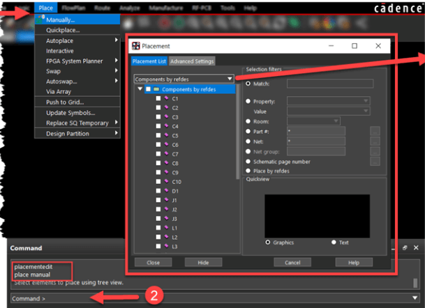
2.2 PCB Layout (Allegro PCB Editor)
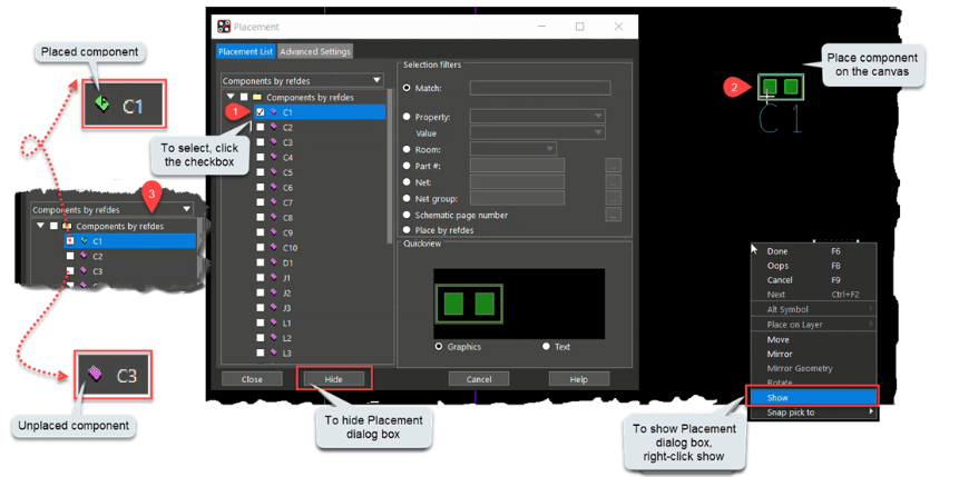
- The schematic is imported into Allegro PCB Editor for physical board design.
- Component Placement: Critical components (e.g., processors, memory) are placed first, followed by supporting parts.
- Routing: Manual, semi-automatic, and automatic routing options are available. High-speed signals require controlled impedance routing.
- Design Rule Checking (DRC): Ensures compliance with spacing, clearance, and manufacturing constraints.
2.3 Signal and Power Integrity Analysis
- Allegro Sigrity or Allegro SI/PI tools analyze signal reflections, crosstalk, and power delivery.
- Engineers optimize trace widths, layer stackup, and decoupling capacitors to minimize noise.
2.4 3D Visualization and Mechanical Integration
- Allegro’s 3D Canvas allows designers to visualize the PCB in a real-world enclosure.
- Collision detection ensures components do not interfere with mechanical parts.
2.5 Manufacturing Output
- Final design files (Gerber, NC drill, pick-and-place) are generated for fabrication.
- Allegro supports DFM (Design for Manufacturability) checks to avoid production issues.
3. Advantages of Using Cadence Allegro
3.1 High Performance for Complex Designs
Allegro excels in handling high-speed, multi-layer PCBs with thousands of components. Its advanced routing algorithms ensure efficient trace management.
3.2 Constraint-Driven Methodology
Designers can enforce electrical, thermal, and mechanical constraints, reducing errors and improving reliability.
3.3 Integration with Other Cadence Tools
Allegro seamlessly integrates with:
- OrCAD Capture for schematic entry.
- Sigrity for signal integrity analysis.
- Clarity 3D Solver for electromagnetic simulations.
3.4 Collaboration and Team Design
Allegro supports team-based design with features like partitioning and concurrent editing, allowing multiple engineers to work on the same PCB simultaneously.
3.5 Industry-Standard Outputs
Allegro generates files compatible with all major PCB manufacturers, ensuring smooth production transitions.
4. Best Practices for PCB Design in Allegro
To maximize efficiency and avoid common pitfalls, designers should follow these best practices:
4.1 Organize Component Libraries
- Maintain a well-structured library with verified footprints and symbols.
- Use Allegro’s CIS for centralized component management.
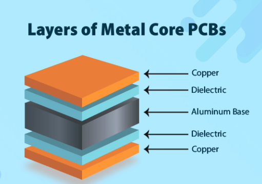
4.2 Optimize Layer Stackup
- Define proper dielectric materials and copper weights for impedance control.
- Use ground and power planes to minimize noise.
4.3 Use Constraints Early
- Set up differential pairs, length matching, and spacing rules before routing.
- Apply high-speed design rules for critical signals (e.g., DDR, PCIe).
4.4 Perform Regular DRC Checks
- Run Design Rule Checks at every major design phase to catch errors early.
4.5 Simulate Before Finalizing
- Use Allegro SI/PI to validate signal integrity and power distribution.
5. Conclusion
Cadence Allegro is a powerful, industry-proven PCB design solution that caters to the needs of modern electronics. Its robust features—ranging from schematic capture to 3D visualization—make it indispensable for high-speed and high-density PCB designs. By following structured workflows and best practices, engineers can leverage Allegro to create reliable, manufacturable, and high-performance circuit boards.
As PCB technology evolves with higher speeds, smaller form factors, and increased complexity, tools like Allegro will continue to play a crucial role in shaping the future of electronics design.