PCB Digital IO Modules: Daisy-Chain Design and Signal Integrity Tactics
Key Takeaways
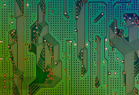
When designing daisy-chained PCB digital I/O modules, balancing signal integrity with pcb manufacturing cost requires strategic planning. Start by ensuring your RS485 bus integration minimizes signal reflections—this means matching impedance across all nodes and keeping trace lengths consistent. For two-layer board designs, prioritize a continuous ground plane to reduce noise and stabilize reference voltages, especially when working with high-speed digital signals.
Relay outputs demand careful routing to avoid coupling noise into sensitive analog or digital lines. Use star topologies for power distribution in daisy-chained modules, and separate analog/digital grounds with a single-point connection. Partnering with experienced pcb manufacturing companies ensures your design adheres to industrial-grade tolerances, which is critical for minimizing errors like crosstalk or voltage drops.
| Design Consideration | Impact on Performance |
|---|---|
| Continuous ground plane | Reduces EMI and noise |
| Proper power routing | Prevents voltage drops |
| RS485 termination | Eliminates signal reflections |
Always validate your layout through signal integrity simulations and real-world testing. For example, check industrial communication standards to ensure compliance. Remember, overlooking pcb manufacturing business constraints—like minimum trace widths or material choices—can escalate costs or delay production. By addressing these factors early, you’ll create robust systems that perform reliably in harsh environments.
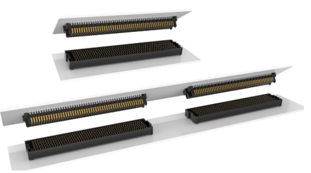
RS485 Daisy-Chain PCB Design Tactics
When designing RS485 daisy-chain configurations for PCB digital I/O modules, precise component placement and trace routing are critical. Start by positioning transceivers close to connectors to minimize stub lengths, which reduces signal reflections. Use differential pair routing with controlled impedance (typically 120Ω for RS485) and ensure traces maintain consistent spacing to avoid crosstalk. Termination resistors should be placed at both ends of the bus to eliminate reflections, but omit them on intermediate nodes to preserve signal integrity.
Tip: For multi-node systems, prioritize a single continuous ground plane to provide a low-impedance return path. Split planes can introduce noise, especially in high-speed industrial environments.
When collaborating with PCB manufacturing companies, clarify your stack-up requirements early. A two-layer board often suffices for simpler designs, but ensure the ground plane covers at least 75% of the bottom layer to reduce EMI. For cost-sensitive projects, discuss PCB manufacturing cost optimization strategies—such as panelization or standard material selection—without compromising the 3.3mm trace-to-edge clearance needed for isolation.
If your PCB manufacturing business involves high-volume production, validate prototypes for skew tolerance and common-mode noise rejection. Use simulation tools to model signal behavior across the daisy chain, particularly at frequencies above 10MHz. Pair this with physical testing under industrial noise conditions to ensure compliance with RS485 standards like TIA/EIA-485-A.
Finally, integrate TVS diodes near connectors for transient protection, and route power traces away from differential pairs to avoid inductive coupling. By balancing design rigor with PCB manufacturing feasibility, you can achieve reliable daisy-chain performance even in electrically harsh environments.
Two-Layer Board Ground Plane Strategies
When designing PCB digital I/O modules with a two-layer stackup, your ground plane strategy directly impacts signal integrity and noise immunity. Start by dedicating the bottom layer as a continuous ground plane—this minimizes loop inductance and provides a stable reference for high-speed signals like those in RS485 bus configurations. Avoid splitting the ground plane unnecessarily, as fragmented return paths can introduce electromagnetic interference (EMI), especially in daisy-chained systems. If splits are unavoidable (e.g., for power routing), ensure they’re perpendicular to critical signal traces to reduce coupling.
For pcb manufacturing companies, balancing pcb manufacturing cost with performance is key. Two-layer designs are cost-effective but require disciplined layout practices. Use ground stitching vias near connector pins and between digital I/O sections to maintain low impedance across the plane. This becomes critical when integrating relay outputs or mixed-signal components, where ground bounce can disrupt logic levels. When collaborating with pcb manufacturing business partners, clarify copper weight and spacing tolerances to ensure the ground plane’s conductivity meets industrial-grade requirements.
Finally, pair your ground plane with a star topology for power distribution to avoid ground loops. This approach, combined with proper decoupling capacitors near ICs, stabilizes supply voltages and reduces noise—a non-negotiable for reliable pcb digital systems operating in harsh environments.
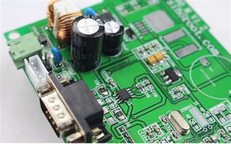
Relay Output Configuration Best Practices
When implementing relay output configurations in industrial-grade digital I/O modules, prioritize isolation between control logic and high-power circuits. Use PCB manufacturing techniques like split ground planes to separate sensitive analog signals from relay switching noise, ensuring compliance with EMI standards. For multi-channel designs, maintain at least 3-4mm clearance between adjacent relay traces to prevent cross-talk—a critical factor in PCB manufacturing cost optimization, as tighter spacing often requires advanced fabrication processes.
Opt for low-resistance copper pours under relay contacts to dissipate heat efficiently, especially when driving inductive loads. Partner with experienced PCB manufacturing companies to validate thermal relief patterns and pad sizes, as improper designs may lead to solder joint fatigue during thermal cycling. Incorporate snubber circuits (RC networks) across relay coils to suppress voltage spikes, protecting downstream components in daisy-chained systems.
When selecting relays, verify their mechanical endurance ratings against your application’s switching frequency. For PCB manufacturing business stakeholders, balancing relay quality with board real estate constraints directly impacts system longevity and maintenance costs. Always prototype with your fabricator to test relay actuation timing against signal propagation delays in RS485 networks, ensuring synchronized operation across the chain.

Signal Integrity Optimization for Digital I/O
When designing PCB digital I/O modules, maintaining signal integrity requires balancing layout precision and electrical performance. Start by ensuring controlled impedance traces for high-speed signals, especially when integrating RS485 buses in daisy-chain configurations. Use ground planes to minimize noise coupling—on two-layer boards, dedicate one layer to a continuous ground reference, stitching vias near critical components to reduce loop inductance.
Avoid parallel routing of digital and power traces; instead, separate them by at least 3x the trace width. For relay outputs, place suppression diodes close to inductive loads to clamp voltage spikes. Partnering with experienced PCB manufacturing companies ensures stack-up accuracy, which directly impacts PCB manufacturing cost and signal performance.
When optimizing for industrial applications, consider termination resistors at both ends of RS485 lines to prevent reflections. Use differential pair routing with matched lengths to maintain timing alignment. If your PCB manufacturing business involves high-volume production, validate designs through pre-production simulations to identify crosstalk risks early. Finally, test prototypes under real-world noise conditions—this step often reveals gaps that theoretical models miss.
Power Routing in Daisy-Chained Modules
When designing PCB digital I/O modules in daisy-chain configurations, managing power routing requires balancing efficiency and reliability. Start by calculating voltage drop across the chain, especially when modules draw power sequentially. Use wider traces (≥20 mil) for high-current paths to minimize resistive losses—a critical factor in pcb manufacturing cost optimization. For multi-module systems, consider star-topology branches from a central power node to ensure uniform voltage distribution, avoiding cascading failures.
Incorporate a dedicated ground plane to stabilize return paths, but isolate digital and relay power domains to prevent noise coupling. This separation becomes vital when integrating relay outputs, as switching transients can disrupt sensitive RS485 bus signals. Partnering with experienced pcb manufacturing companies ensures proper layer stack-up and via placement for thermal management, particularly in industrial environments.
Decoupling capacitors (e.g., 100nF ceramic + 10μF electrolytic) should be placed as close as possible to each module’s power pins. For longer chains, local regulation at intermediate nodes helps maintain voltage thresholds. When prototyping, validate your design with pcb manufacturing business experts to identify bottlenecks like via current capacity or copper weight limitations. Remember, inefficient power routing not only escalates pcb manufacturing expenses but also risks premature component degradation in field applications. Always simulate worst-case load scenarios before finalizing the layout.
Industrial-Grade RS485 Bus Integration Tips
When integrating RS485 buses into industrial environments, you’ll need to balance robust pcb manufacturing practices with precise electrical design. Start by ensuring proper termination at both ends of the daisy chain to minimize signal reflections—a critical step for maintaining signal integrity in noisy settings. Use differential pair routing with matched trace lengths to preserve the RS485’s noise immunity, and avoid parallel runs near high-voltage traces or motor drivers.
For reliable performance, collaborate with experienced pcb manufacturing companies that specialize in industrial-grade materials. They can optimize layer stack-ups to isolate the RS485 bus from power planes, reducing capacitive coupling. If you’re constrained by pcb manufacturing cost, prioritize a two-layer design with a continuous ground plane beneath signal traces. This shields against electromagnetic interference (EMI) while simplifying fabrication—a key consideration for scaling a pcb manufacturing business.
Always validate your layout with impedance testing, targeting 120Ω for RS485 networks. Incorporate TVS diodes or transient suppressors near connectors to protect against voltage spikes, and ensure all nodes share a common reference ground. By aligning these strategies with industrial standards like IEC 61000, you’ll achieve predictable signal behavior even in harsh operating conditions.
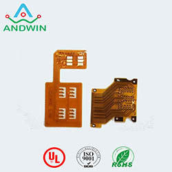
Avoiding Common PCB Digital Design Errors
When designing PCB digital I/O modules, overlooking foundational principles can lead to costly revisions during pcb manufacturing. A frequent mistake involves improper grounding—failing to maintain a continuous ground plane on two-layer boards creates return path discontinuities, amplifying electromagnetic interference (EMI). You’ll want to prioritize star grounding for sensitive components like RS485 transceivers while avoiding ground loops in daisy-chain configurations.
Another pitfall lies in trace routing: neglecting controlled impedance for high-speed signals or mismatching trace lengths between daisy-chained modules introduces timing skew. Always maintain at least 3x the trace width as clearance between digital lines to minimize crosstalk. For pcb manufacturing companies, these errors often result in increased pcb manufacturing cost due to added test cycles or material waste from impedance mismatches.
Don’t underestimate power distribution either. Insufficient decoupling capacitor placement near digital ICs causes voltage droops during simultaneous switching events—critical in systems with multiple relay outputs. Use bulk capacitors at power entry points and pair them with 100nF ceramic capacitors at each IC’s VCC pin.
Finally, collaborate early with your pcb manufacturing business partner to validate stack-up materials. Subpar dielectric constants or copper roughness can degrade signal integrity, particularly in industrial environments with extended temperature ranges. By addressing these errors proactively, you reduce respins and ensure robust performance across your daisy-chain network.
Testing Protocols for Reliable Daisy-Chain Systems
When validating PCB digital daisy-chain systems, start with impedance testing to confirm trace characteristics match RS485 requirements. Use time-domain reflectometry (TDR) to identify discontinuities caused by improper trace geometry or via placement—common issues in pcb manufacturing workflows. Next, perform signal integrity checks under load conditions, monitoring for crosstalk or reflections that degrade performance in multi-drop configurations.
Collaborate with pcb manufacturing companies to verify stack-up tolerances, especially for two-layer boards where ground plane integrity directly impacts noise immunity. Automated continuity testing ensures all nodes in the daisy-chain are correctly linked, minimizing assembly errors that escalate pcb manufacturing cost during rework. For relay outputs, validate switching thresholds using programmable loads to simulate industrial environments.
Incorporate boundary scan (JTAG) testing to isolate faults in densely routed designs, a critical step when balancing pcb manufacturing business priorities like yield and turnaround time. Finally, conduct end-to-end bus communication tests with varying cable lengths and termination schemes to replicate real-world operating margins. Documenting these protocols not only streamlines compliance but also reduces field failures, aligning with lifecycle cost objectives for industrial-grade systems.
Conclusion
When designing PCB digital I/O modules for daisy-chain configurations, balancing signal integrity with pcb manufacturing cost requires strategic planning. Your choices in layout—such as prioritizing a continuous ground plane on two-layer boards—directly influence noise immunity and long-term reliability. Partnering with experienced pcb manufacturing companies ensures your design aligns with industrial-grade tolerances, especially for RS485 bus integration and relay output placements.
To minimize errors, validate power routing paths early and simulate signal degradation risks under worst-case scenarios. This proactive approach reduces rework costs, a critical factor in the pcb manufacturing business where iterative revisions impact timelines. Testing protocols like impedance checks and daisy-chain loop validation further safeguard against field failures.
Ultimately, optimizing for pcb manufacturing efficiency means balancing performance with scalability. By embedding grounding strategies and bus termination practices into your design workflow, you create systems that withstand industrial demands while keeping production costs predictable. Whether refining prototypes or scaling production, these principles ensure your digital I/O modules deliver consistent performance across complex daisy-chain networks.
FAQs
How does daisy-chain design affect signal integrity in PCB digital I/O modules?
Daisy-chain configurations introduce challenges like cumulative noise and impedance mismatches. To maintain signal integrity, prioritize short trace lengths between nodes, use termination resistors, and ensure proper ground plane continuity. Partnering with experienced pcb manufacturing companies helps optimize stack-up designs for controlled impedance.
What role do two-layer boards play in reducing pcb manufacturing cost?
Two-layer designs simplify fabrication, lowering pcb manufacturing cost compared to multi-layer alternatives. However, ensure adequate ground fills and strategic component placement to minimize EMI. Reputable pcb manufacturing providers can advise on balancing cost and performance for industrial-grade reliability.
How do relay outputs impact power routing in daisy-chained systems?
Relay outputs require isolated traces to prevent back-EMF interference. Route high-current paths away from sensitive digital signals, and use separate ground returns. For complex layouts, consult pcb manufacturing business experts to validate thermal management and creepage/clearance margins.
Why is RS485 bus integration critical for industrial applications?
RS485’s differential signaling enhances noise immunity in electrically harsh environments. Implement twisted-pair routing and shield connections to chassis ground. When prototyping, verify compatibility with your pcb manufacturing partner’s capabilities for impedance-controlled boards.
Need Custom Solutions for Your PCB Project?
Optimize your daisy-chain designs with professional support—please click here to explore https://www.andwinpcb.com/pcb-manufacturing/ for tailored pcb manufacturing services.