PCB Grounding and Decoupling: Fundamental Concepts and Best Practices
Introduction
Printed Circuit Board (PCB) design is a critical aspect of electronic system development, and proper grounding and decoupling techniques are essential for ensuring signal integrity, reducing noise, and improving overall system performance. Poor grounding and inadequate decoupling can lead to electromagnetic interference (EMI), power supply fluctuations, and signal degradation, which may result in malfunctioning circuits.
This article explores the fundamental principles of PCB grounding and decoupling, discussing key concepts, common challenges, and best practices to optimize PCB performance.
1. Understanding PCB Grounding
Grounding in PCB design refers to the method of providing a common reference point (ground plane) for electrical circuits to ensure stable voltage levels and minimize noise. A well-designed grounding system helps in:
- Reducing electromagnetic interference (EMI).
- Preventing ground loops.
- Ensuring signal integrity.
- Improving power distribution.
1.1 Types of Grounding Schemes
Several grounding techniques are used in PCB design, each with its advantages and limitations.
(A) Single-Point Grounding
- All ground connections are tied to a single physical location.
- Best for low-frequency circuits (<1 MHz) to avoid ground loops.
- Disadvantage: High-frequency signals may suffer due to increased impedance.
(B) Multi-Point Grounding
- Ground connections are made at multiple points, typically using a ground plane.
- Suitable for high-frequency circuits (>10 MHz) to minimize impedance.
- Disadvantage: Risk of ground loops if not properly managed.
(C) Hybrid Grounding
- Combines single-point and multi-point grounding.
- Uses inductors or capacitors to isolate different ground sections at certain frequencies.
- Common in mixed-signal (analog + digital) designs.
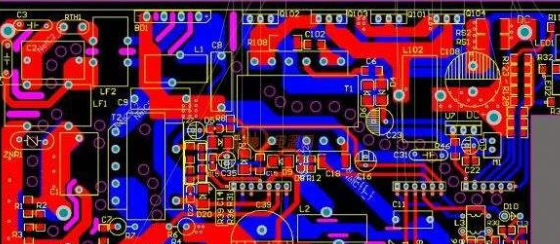
1.2 Ground Plane Design
A ground plane is a large conductive area (usually copper) that serves as a low-impedance return path for signals. Key considerations include:
- Solid Ground Plane: Provides the lowest impedance and best EMI shielding.
- Split Ground Planes: Used in mixed-signal designs to separate analog and digital grounds, but must be connected at a single point to avoid noise coupling.
- Avoiding Ground Loops: Ensure that ground paths do not form loops that can pick up EMI.
2. Decoupling in PCB Design
Decoupling refers to the use of capacitors to stabilize power supply voltages by filtering high-frequency noise. It is crucial for:
- Maintaining stable power delivery to ICs.
- Reducing voltage fluctuations caused by switching circuits.
- Minimizing radiated and conducted EMI.
2.1 Why Decoupling is Necessary
When digital ICs switch states, they draw sudden bursts of current, causing transient voltage drops (known as “ground bounce” or “power droop”). Decoupling capacitors provide localized energy storage to compensate for these fluctuations.
2.2 Types of Decoupling Capacitors
Different capacitors serve different frequency ranges:
| Capacitor Type | Typical Value | Effective Frequency Range | Purpose |
|---|---|---|---|
| Bulk Capacitor | 10µF – 100µF | Low-frequency (<1 MHz) | Stabilizes power supply |
| Ceramic Capacitor | 0.1µF – 1µF | Mid-frequency (1 MHz – 100 MHz) | Primary decoupling for ICs |
| High-Frequency Capacitor | 1nF – 10nF | High-frequency (>100 MHz) | Handles fast transients |
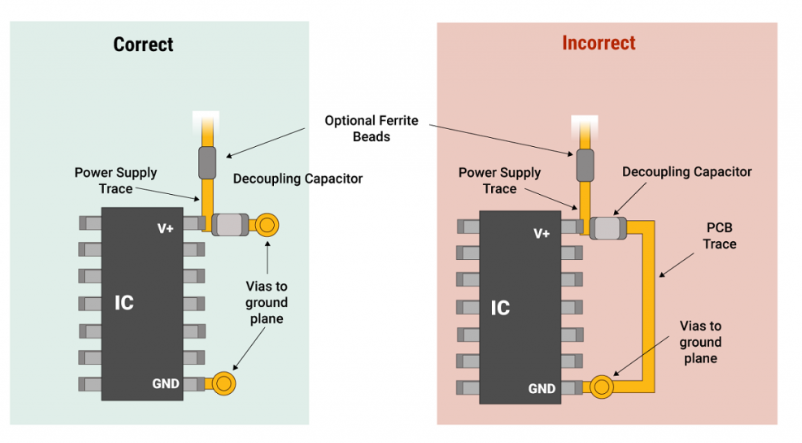
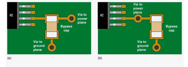
2.3 Placement of Decoupling Capacitors
- Close to Power Pins: Place decoupling capacitors as close as possible to the IC’s power pins to minimize parasitic inductance.
- Multiple Capacitors in Parallel: Use a combination of different capacitor values to cover a wide frequency range.
- Minimize Loop Area: Keep traces short between the capacitor, power pin, and ground to reduce inductance.
3. Common Grounding and Decoupling Mistakes
Several common errors can degrade PCB performance:
3.1 Improper Ground Plane Splitting
- Splitting ground planes without proper stitching can increase EMI.
- Solution: Use a unified ground plane with careful component placement.
3.2 Insufficient Decoupling
- Using only one large capacitor instead of multiple smaller ones.
- Solution: Follow the “rule of thumb” – use at least one 0.1µF capacitor per power pin.
3.3 Long Decoupling Traces
- Long traces introduce parasitic inductance, reducing capacitor effectiveness.
- Solution: Place capacitors directly adjacent to power pins.
3.4 Ignoring Return Paths
- High-speed signals require a clear return path under the signal trace.
- Solution: Ensure a continuous ground plane beneath signal traces.
4. Best Practices for Optimal PCB Grounding and Decoupling
To achieve a robust PCB design, follow these guidelines:
4.1 Grounding Best Practices
- Use a solid ground plane whenever possible.
- Separate analog and digital grounds only when necessary, and connect them at a single point.
- Avoid ground loops by ensuring a star grounding topology for sensitive circuits.
- Use vias to connect components to the ground plane with minimal impedance.
4.2 Decoupling Best Practices
- Use multiple capacitors (e.g., 10µF, 0.1µF, and 0.01µF) near each IC.
- Place high-frequency decoupling capacitors closest to the power pins.
- Minimize trace lengths between capacitors and ICs.
- Simulate power distribution networks (PDN) to verify decoupling effectiveness.
4.3 Mixed-Signal PCB Considerations
- Keep analog and digital sections physically separated.
- Use a single ground plane with careful partitioning rather than splitting.
- Route high-speed digital signals away from sensitive analog traces.
5. Conclusion
Proper grounding and decoupling are fundamental to PCB design, ensuring signal integrity, reducing noise, and preventing power-related issues. By understanding the different grounding schemes, selecting appropriate decoupling capacitors, and following best practices, designers can optimize PCB performance and reliability.
As electronic systems continue to evolve with higher speeds and greater complexity, mastering these foundational concepts becomes even more critical. Implementing robust grounding and decoupling strategies will lead to more stable, efficient, and noise-resistant PCB designs.