Pcb manufacturing facility
Optimizing Workflow in a PCB Manufacturing Facility
Optimizing workflow in a PCB manufacturing facility is a multifaceted endeavor that requires a strategic approach to enhance efficiency, reduce costs, and maintain high-quality standards.
The first step in this optimization process involves a thorough analysis of the current workflow.
By mapping out each stage of production, from the initial design phase to the final quality control checks, facility managers can identify bottlenecks and areas where improvements can be made. This comprehensive understanding of the workflow is crucial for implementing effective changes.
One of the primary strategies for optimizing workflow is the adoption of advanced manufacturing technologies.
Automation plays a significant role in this regard, as it can significantly reduce the time and labor required for repetitive tasks. For instance, automated pick-and-place machines can precisely position components on the PCB, thereby increasing accuracy and speed. Additionally, the integration of computer-aided design (CAD) and computer-aided manufacturing (CAM) systems can streamline the transition from design to production, ensuring that designs are accurately translated into physical products.
Moreover, the implementation of lean manufacturing principles can greatly enhance workflow efficiency.
Lean manufacturing focuses on minimizing waste and maximizing value by optimizing processes and eliminating non-essential activities. Techniques such as Just-In-Time (JIT) production, where materials are ordered and received only as they are needed, can reduce inventory costs and minimize storage space requirements. Furthermore, continuous improvement practices, such as Kaizen, encourage employees to regularly suggest and implement incremental changes that can lead to significant long-term improvements.
Another critical aspect of optimizing workflow in a PCB manufacturing facility is effective communication and collaboration among different departments.
Ensuring that design, production, and quality control teams are in constant communication can prevent misunderstandings and errors that could disrupt the workflow. Utilizing integrated software systems that allow for real-time updates and information sharing can facilitate this communication. For example, enterprise resource planning (ERP) systems can provide a centralized platform for tracking production schedules, inventory levels, and order statuses, thereby enhancing coordination and reducing delays.
In addition to technological and procedural improvements, workforce training and development are essential for optimizing workflow.
Employees must be well-versed in the latest manufacturing techniques and technologies to operate efficiently. Regular training sessions and workshops can help keep the workforce updated on best practices and new advancements in the field. Moreover, fostering a culture of continuous learning and improvement can motivate employees to take initiative and contribute to the optimization process.
Quality control is another vital component of an optimized workflow.
Implementing rigorous quality assurance protocols at various stages of production can help identify and rectify defects early, preventing costly rework and ensuring that the final products meet the required standards. Automated optical inspection (AOI) systems, for example, can quickly and accurately detect defects in PCBs, allowing for immediate corrective actions.
Finally, data analysis and performance monitoring are crucial for sustaining an optimized workflow.
By collecting and analyzing data on production metrics, such as cycle times, defect rates, and equipment utilization, facility managers can gain insights into the effectiveness of their optimization efforts. This data-driven approach enables continuous monitoring and adjustment of processes to maintain optimal performance.
In conclusion, optimizing workflow in a PCB manufacturing facility involves a combination of technological advancements, lean manufacturing principles, effective communication, workforce training, rigorous quality control, and data analysis. By systematically addressing each of these areas, facility managers can create a more efficient, cost-effective, and high-quality production environment.
Latest Technological Advancements in PCB Manufacturing
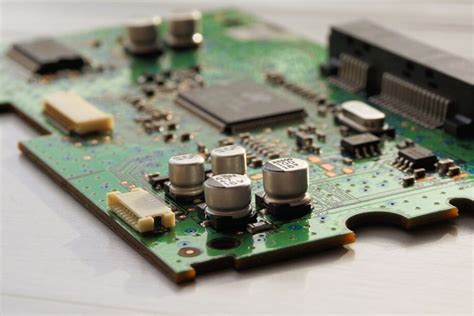
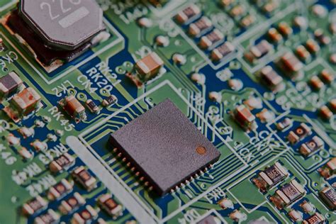
The field of printed circuit board (PCB) manufacturing has witnessed significant technological advancements in recent years, driven by the increasing demand for more efficient, compact, and reliable electronic devices. One of the most notable advancements is the development of high-density interconnect (HDI) technology. HDI PCBs are characterized by their higher wiring density per unit area, which is achieved through the use of finer lines and spaces, smaller vias, and capture pads. This technology allows for more components to be placed on both sides of the PCB, thereby reducing the overall size of the board and enhancing its performance. Consequently, HDI technology has become indispensable in the production of modern electronic devices such as smartphones, tablets, and wearable technology.
In addition to HDI technology, the advent of flexible PCBs has revolutionized the industry.
Flexible PCBs, made from materials such as polyimide or polyester film, offer the advantage of being able to bend and fold without breaking. This flexibility enables the design of more compact and versatile electronic devices, which is particularly beneficial in applications where space is limited or where the PCB needs to conform to a specific shape. Moreover, flexible PCBs are known for their durability and resistance to harsh environmental conditions, making them ideal for use in automotive, medical, and aerospace industries.
Another significant advancement in PCB manufacturing is the implementation of advanced materials.
Traditional PCBs are typically made from fiberglass-reinforced epoxy laminates, but recent developments have introduced materials such as ceramic and metal-core PCBs. Ceramic PCBs offer superior thermal conductivity and electrical insulation, making them suitable for high-power applications. Metal-core PCBs, on the other hand, provide excellent heat dissipation, which is crucial for maintaining the performance and longevity of electronic components. These advanced materials not only enhance the functionality of PCBs but also open up new possibilities for their application in various industries.
Furthermore, the integration of automation and artificial intelligence (AI) in PCB manufacturing processes has significantly improved efficiency and precision.
Automated optical inspection (AOI) systems, for instance, use high-resolution cameras and AI algorithms to detect defects in PCBs with remarkable accuracy. This technology not only reduces the likelihood of human error but also speeds up the inspection process, ensuring that only high-quality PCBs are delivered to customers. Additionally, AI-driven design software has made it possible to optimize PCB layouts for better performance and manufacturability, thereby reducing the time and cost associated with the design process.
Moreover, advancements in additive manufacturing, commonly known as 3D printing, have also made their mark on the PCB industry.
3D printing allows for the creation of complex PCB structures that would be difficult or impossible to achieve with traditional manufacturing methods. This technology enables rapid prototyping and customization, allowing manufacturers to quickly iterate on designs and bring new products to market faster. Additionally, 3D-printed PCBs can incorporate unique features such as embedded components and intricate geometries, further expanding the possibilities for electronic device design.
In conclusion, the latest technological advancements in PCB manufacturing have significantly enhanced the capabilities and applications of PCBs.
From HDI and flexible PCBs to advanced materials and AI-driven processes, these innovations have paved the way for more efficient, compact, and reliable electronic devices. As the demand for cutting-edge technology continues to grow, it is expected that the PCB manufacturing industry will continue to evolve, driven by ongoing research and development efforts aimed at pushing the boundaries of what is possible.
Quality Control Measures in PCB Production
In the realm of printed circuit board (PCB) manufacturing, quality control measures are paramount to ensuring the reliability and performance of the final product. The intricate nature of PCBs, which serve as the backbone of virtually all electronic devices, necessitates a rigorous approach to quality assurance. This begins with the selection of raw materials, where only high-grade substrates, copper foils, and laminates are chosen to form the foundation of the PCB. By starting with superior materials, manufacturers can mitigate potential defects that could arise later in the production process.
As the manufacturing process commences, each stage is meticulously monitored.
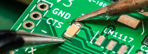
During the initial phase of photolithography, where the circuit pattern is transferred onto the substrate, precision is critical. Any deviation can lead to misalignment, which could compromise the functionality of the PCB. To prevent such issues, advanced imaging systems are employed to ensure that the patterns are accurately replicated. These systems use high-resolution cameras and sophisticated software to detect even the slightest discrepancies, allowing for immediate corrections.
Following photolithography, the etching process removes unwanted copper to reveal the desired circuit paths.
Here, chemical control is essential. The concentration and temperature of the etching solution must be carefully regulated to achieve consistent results. Automated systems are often used to monitor these parameters in real-time, ensuring that the etching process proceeds uniformly across all boards. Additionally, periodic sampling and testing of the etched boards are conducted to verify that the copper removal is precise and that the circuit paths are intact.
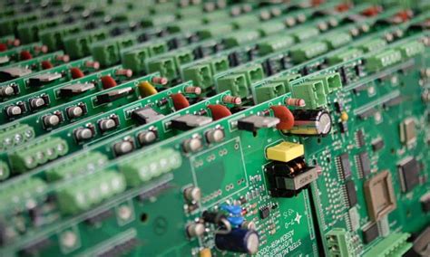
Once the etching is complete, the boards undergo a series of inspections.
Optical inspection systems play a crucial role at this stage, scanning the boards for any visual defects such as scratches, pits, or incomplete etching. These systems are capable of identifying flaws that may not be visible to the naked eye, thus enhancing the overall quality control process. Furthermore, automated optical inspection (AOI) machines are employed to compare the actual board against the intended design, highlighting any discrepancies that need to be addressed.
The next critical step involves the application of solder mask and silkscreen.
The solder mask, which protects the copper traces from oxidation and prevents solder bridges during component assembly, must be applied uniformly. Any irregularities in the solder mask can lead to short circuits or other failures. To ensure uniform application, manufacturers use precision coating equipment and conduct thorough inspections to verify coverage and adhesion. Similarly, the silkscreen, which provides component labels and other markings, must be applied with high accuracy to ensure readability and proper component placement.
Electrical testing is another vital component of quality control in PCB production.
This involves subjecting the boards to various electrical tests to confirm that all connections are correct and that there are no shorts or open circuits. Flying probe testers and bed-of-nails testers are commonly used for this purpose, providing a comprehensive assessment of the board’s electrical integrity. These tests are crucial for identifying any latent defects that could affect the board’s performance in the field.
Finally, before the PCBs are shipped to customers, they undergo a final inspection and testing phase.
This includes a visual inspection to check for any remaining defects, as well as functional testing to ensure that the boards operate as intended. By implementing these stringent quality control measures throughout the manufacturing process, PCB manufacturers can deliver products that meet the highest standards of reliability and performance, thereby ensuring customer satisfaction and maintaining their reputation in the industry.
Sustainability Practices in PCB Manufacturing Facilities
Sustainability practices in PCB manufacturing facilities have become increasingly important as the industry seeks to balance technological advancement with environmental responsibility. The production of printed circuit boards (PCBs) involves various processes that can have significant environmental impacts, including the use of hazardous chemicals, substantial water consumption, and the generation of electronic waste. Consequently, manufacturers are adopting a range of sustainability practices to mitigate these effects and promote a more eco-friendly approach to PCB production.
One of the primary areas of focus in sustainable PCB manufacturing is the reduction of hazardous substances.
Traditional PCB production often involves the use of toxic chemicals such as lead, mercury, and cadmium, which pose significant risks to both human health and the environment. To address this, many facilities are transitioning to lead-free soldering processes and using alternative materials that are less harmful. For instance, the adoption of RoHS (Restriction of Hazardous Substances) compliant materials has become a standard practice, ensuring that the components used in PCBs meet stringent environmental and safety criteria.
In addition to reducing hazardous substances, PCB manufacturers are also implementing measures to minimize water usage and improve water management.
The production process typically requires large volumes of water for cleaning and rinsing PCBs, which can lead to substantial water waste. To combat this, facilities are investing in advanced water recycling and treatment systems. These systems allow for the reuse of water within the manufacturing process, significantly reducing the overall consumption and minimizing the discharge of contaminated water into the environment. By implementing closed-loop water systems, manufacturers can achieve a more sustainable and efficient use of this vital resource.
Energy efficiency is another critical aspect of sustainability in PCB manufacturing.
The production process is energy-intensive, involving high-temperature operations such as soldering and lamination. To reduce energy consumption, facilities are adopting energy-efficient equipment and optimizing their production processes. For example, the use of energy-efficient ovens and reflow soldering machines can significantly lower the energy required for these operations. Additionally, manufacturers are exploring renewable energy sources, such as solar and wind power, to further reduce their carbon footprint. By integrating these energy-saving measures, PCB manufacturing facilities can decrease their reliance on non-renewable energy sources and contribute to a more sustainable industry.
Waste management is also a key component of sustainability practices in PCB manufacturing.
The production process generates various types of waste, including scrap materials, defective PCBs, and packaging waste. To address this, manufacturers are implementing comprehensive waste reduction and recycling programs. By optimizing material usage and improving production yields, facilities can minimize the generation of scrap and defective products.
Furthermore, recycling initiatives for materials such as copper, aluminum, and plastic help to divert waste from landfills and promote the reuse of valuable resources. These efforts not only reduce the environmental impact of PCB manufacturing but also contribute to cost savings and resource efficiency.
In conclusion, sustainability practices in PCB manufacturing facilities are essential for reducing the environmental impact of the industry. By focusing on the reduction of hazardous substances, improving water management, enhancing energy efficiency, and implementing effective waste management strategies, manufacturers can create a more sustainable and responsible production process. As the demand for electronic devices continues to grow, the adoption of these practices will play a crucial role in ensuring that the PCB manufacturing industry can meet this demand while minimizing its ecological footprint.