Pcb manufacturing guidelines
Best Practices For PCB manufacturing guidelines
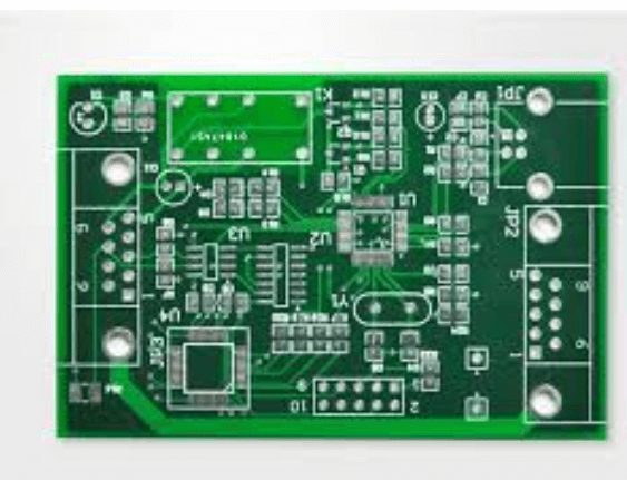
In the realm of electronics, the design and layout of Printed Circuit Boards (PCBs) are critical to the functionality and reliability of the final product. Adhering to best practices in PCB design layout not only ensures optimal performance but also mitigates potential issues during manufacturing and operation. To achieve a high-quality PCB, several key guidelines must be followed meticulously.
First and foremost, component placement is a fundamental aspect of PCB design.
Proper placement of components can significantly influence the board’s performance and manufacturability. It is advisable to place components in a logical sequence, starting with connectors, followed by power circuits, precision circuits, and finally, the rest of the components. This systematic approach facilitates easier routing and minimizes the risk of interference. Additionally, maintaining adequate spacing between components is crucial to prevent short circuits and ensure sufficient heat dissipation.
Transitioning to the topic of signal integrity, it is essential to consider the routing of traces.
High-speed signals should be routed with care to avoid issues such as crosstalk and signal degradation. Utilizing differential pairs for high-speed signals can help maintain signal integrity. Moreover, keeping trace lengths as short as possible and avoiding sharp angles can reduce signal reflections and impedance mismatches. Implementing controlled impedance routing for critical signals is another best practice that can enhance the overall performance of the PCB.
Power distribution is another critical aspect that demands attention.
A well-designed power distribution network ensures that all components receive stable and adequate power. Utilizing power planes, rather than traces, can provide a low-impedance path for power delivery and reduce voltage drops. Decoupling capacitors should be strategically placed near power pins of integrated circuits to filter out noise and stabilize the power supply. Additionally, separating analog and digital grounds can prevent noise from digital circuits from affecting sensitive analog components.
Thermal management is a vital consideration in PCB design, especially for high-power applications.
Effective thermal management can prevent overheating and extend the lifespan of the components. Incorporating thermal vias, heat sinks, and copper pours can enhance heat dissipation. It is also beneficial to place heat-generating components away from temperature-sensitive ones to avoid thermal interference. Conducting thermal simulations during the design phase can provide insights into potential hotspots and guide the implementation of appropriate cooling strategies.
Design for manufacturability (DFM) is an overarching principle that should be integrated into every stage of PCB design.
Ensuring that the design is manufacturable can reduce production costs and lead times. This includes adhering to the design rules and capabilities of the chosen PCB manufacturer, such as minimum trace widths, spacing, and hole sizes. Additionally, incorporating test points and designing for ease of assembly can facilitate testing and troubleshooting during production.
In conclusion, following best practices in PCB design layout is paramount to achieving a reliable and high-performance product. From strategic component placement and meticulous trace routing to robust power distribution and effective thermal management, each aspect plays a crucial role in the overall success of the PCB. By integrating these guidelines and considering manufacturability throughout the design process, designers can create PCBs that meet both functional and production requirements, ultimately leading to a successful and efficient electronic product.
Essential PCB Material Selection Tips
When embarking on the journey of printed circuit board (PCB) manufacturing, one of the most critical steps is the selection of appropriate materials. The choice of materials can significantly influence the performance, reliability, and cost-effectiveness of the final product. Therefore, understanding the essential guidelines for PCB material selection is paramount for engineers and designers.
To begin with, the substrate material forms the foundation of any PCB.
The most commonly used substrate is FR-4, a composite material made of woven fiberglass cloth with an epoxy resin binder that is flame resistant. FR-4 is favored for its excellent mechanical strength, electrical insulation properties, and cost-effectiveness. However, for high-frequency applications, materials such as Rogers or Teflon (PTFE) are preferred due to their superior dielectric properties and lower signal loss.
Transitioning to the conductive layers, copper is the material of choice for PCB traces due to its excellent electrical conductivity and relatively low cost.
The thickness of the copper layer, often measured in ounces per square foot, is a crucial factor. Standard PCBs typically use 1 oz/ft² copper, but high-power applications may require thicker copper to handle increased current loads and reduce resistive losses.
Another critical consideration is the solder mask, which is a protective layer applied over the copper traces to prevent short circuits and corrosion. The most common material for solder masks is epoxy liquid photoimageable (LPI) solder mask, which offers good adhesion, chemical resistance, and thermal stability. For applications requiring higher precision and finer features, dry film solder masks may be used.
Furthermore, the choice of surface finish on the PCB is essential for ensuring reliable soldering and long-term performance.
Common surface finishes include Hot Air Solder Leveling (HASL), Electroless Nickel Immersion Gold (ENIG), and Organic Solderability Preservative (OSP). HASL is widely used due to its cost-effectiveness and ease of application, but it may not be suitable for fine-pitch components. ENIG, on the other hand, provides a flat surface and excellent solderability, making it ideal for high-density interconnects and fine-pitch components. OSP is a lead-free option that offers good solderability but may have a shorter shelf life compared to other finishes.
In addition to these primary materials, the selection of dielectric materials between the conductive layers is also crucial.
The dielectric constant (Dk) and dissipation factor (Df) of these materials affect signal integrity, especially in high-speed and high-frequency applications. Materials with low Dk and Df values, such as certain types of ceramics or advanced polymers, are preferred for minimizing signal loss and ensuring signal integrity.
Moreover, thermal management is a vital aspect of PCB design, particularly for high-power applications.
Materials with high thermal conductivity, such as metal-core PCBs or thermally conductive laminates, can help dissipate heat more effectively and prevent overheating of components.
Lastly, environmental considerations and regulatory compliance should not be overlooked. The use of lead-free materials and compliance with standards such as RoHS (Restriction of Hazardous Substances) is increasingly important in today’s manufacturing landscape. Selecting materials that meet these requirements ensures that the final product is environmentally friendly and adheres to global regulations.
In conclusion, the selection of materials for PCB manufacturing is a multifaceted process that requires careful consideration of various factors, including electrical performance, thermal management, mechanical strength, and regulatory compliance. By adhering to these essential guidelines, engineers and designers can ensure the production of high-quality, reliable, and cost-effective PCBs that meet the demands of modern electronic applications.
Key Steps In The PCB Fabrication Process
Printed Circuit Board (PCB) manufacturing is a complex process that requires meticulous attention to detail and adherence to specific guidelines to ensure the final product meets the desired specifications. The process begins with the design phase, where engineers use specialized software to create a detailed layout of the circuit.
This layout includes the placement of components, the routing of electrical connections, and the specification of various layers within the PCB.
Once the design is finalized, it is converted into a format suitable for manufacturing, typically Gerber files, which contain all the necessary information for each layer of the PCB.
Following the design phase, the next step is the preparation of the substrate, usually made of fiberglass-reinforced epoxy resin, known as FR4.
This material provides the necessary mechanical support and electrical insulation for the PCB. The substrate is then coated with a thin layer of copper on both sides, which will form the conductive pathways for the electrical signals. The copper-clad substrate is then cleaned and prepared for the application of the photoresist, a light-sensitive material that will be used to transfer the circuit pattern onto the copper surface.
The photoresist-coated substrate is then exposed to ultraviolet (UV) light through a photomask, which contains the circuit pattern.
The areas of the photoresist exposed to the UV light harden, while the unexposed areas remain soft and can be washed away using a developer solution. This process leaves behind a precise pattern of hardened photoresist on the copper surface, which will serve as a protective layer during the subsequent etching process.
Etching is a critical step in PCB fabrication, where the exposed copper areas are removed using a chemical solution, typically ferric chloride or ammonium persulfate. The hardened photoresist protects the desired copper pathways, ensuring that only the unwanted copper is etched away. After etching, the remaining photoresist is stripped away, revealing the final copper circuit pattern on the substrate.
The next phase involves drilling holes for component leads and vias, which are used to connect different layers of the PCB.
Precision drilling machines equipped with carbide drill bits are used to create these holes with high accuracy. Once the drilling is complete, the holes are plated with copper to establish electrical connections between the layers.
Subsequently, the PCB undergoes a process called solder masking, where a protective layer of solder mask is applied to the surface. This layer prevents solder bridges from forming during component assembly and protects the copper traces from oxidation and environmental damage. The solder mask is typically green, although other colors are also available.
The final steps in PCB fabrication include the application of a silkscreen layer, which provides component labels and other important information, and the surface finish, which enhances solderability and protects the exposed copper. Common surface finishes include HASL (Hot Air Solder Leveling), ENIG (Electroless Nickel Immersion Gold), and OSP (Organic Solderability Preservative).
In conclusion, PCB manufacturing involves a series of precise and interrelated steps, each crucial to the overall quality and functionality of the final product. From design and substrate preparation to etching, drilling, and finishing, each phase must be executed with precision and care. By adhering to these guidelines, manufacturers can produce reliable and high-performance PCBs that meet the stringent requirements of modern electronic devices.
Common PCB Manufacturing Mistakes To Avoid
In the realm of electronics, printed circuit boards (PCBs) serve as the backbone of most devices, providing the necessary pathways for electrical currents to flow between components. However, the process of manufacturing PCBs is fraught with potential pitfalls that can compromise the functionality and reliability of the final product. To ensure the highest quality and performance, it is crucial to be aware of common PCB manufacturing mistakes and take steps to avoid them.
One prevalent mistake in PCB manufacturing is inadequate design planning.
This often stems from a lack of thorough understanding of the end-use application and the specific requirements it entails. For instance, failing to consider the thermal management needs of high-power components can lead to overheating and eventual failure. Therefore, it is essential to conduct a comprehensive design review, taking into account factors such as component placement, trace routing, and thermal management strategies.
Another frequent error is the improper selection of materials.
The choice of substrate, copper thickness, and solder mask can significantly impact the board’s performance and durability. For example, using a substrate with insufficient thermal conductivity can result in poor heat dissipation, while an inappropriate solder mask can lead to solder bridging and short circuits. Consequently, it is imperative to select materials that align with the specific requirements of the application and the operating environment.
Transitioning to the manufacturing process itself, one common mistake is the failure to adhere to design for manufacturability (DFM) guidelines.
DFM principles are designed to simplify the manufacturing process and enhance yield rates. Ignoring these guidelines can lead to issues such as misalignment, insufficient solder joints, and difficulty in assembly. To mitigate these risks, it is advisable to collaborate closely with the PCB manufacturer during the design phase to ensure that the design is optimized for production.
Furthermore, inadequate quality control measures can result in defective PCBs reaching the end user.
This can manifest in various forms, such as open circuits, short circuits, and delamination. Implementing rigorous inspection and testing protocols, including automated optical inspection (AOI), X-ray inspection, and electrical testing, can help identify and rectify defects early in the production process. Additionally, maintaining a clean and controlled manufacturing environment is crucial to prevent contamination and ensure the integrity of the PCBs.
Another critical aspect to consider is the accuracy of the Gerber files, which are used to communicate the design specifications to the manufacturer.
Errors in these files, such as incorrect layer alignment or missing drill holes, can lead to significant production delays and increased costs. Therefore, it is essential to meticulously review and verify the Gerber files before submission to the manufacturer.
Moreover, neglecting to account for the tolerances and limitations of the manufacturing equipment can result in boards that do not meet the required specifications. For example, trace widths and spacing that are too fine for the manufacturer’s capabilities can lead to shorts and open circuits. It is important to understand the capabilities and limitations of the manufacturing equipment and design the PCB accordingly.
In conclusion, avoiding common PCB manufacturing mistakes requires a combination of thorough design planning, appropriate material selection, adherence to DFM guidelines, rigorous quality control measures, accurate Gerber file preparation, and consideration of manufacturing equipment limitations. By addressing these factors, manufacturers can enhance the reliability and performance of their PCBs, ultimately leading to more successful electronic products.


