PCB Routing Techniques: A Comprehensive Guide
Introduction
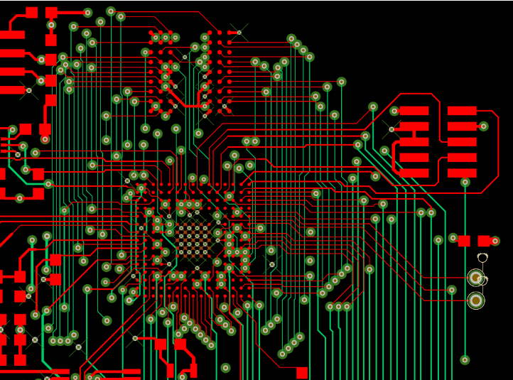
Printed Circuit Board (PCB) design is a critical aspect of electronic product development, and routing (or布线) plays a pivotal role in ensuring signal integrity, power distribution, and electromagnetic compatibility (EMC). Proper routing techniques can significantly impact the performance, reliability, and manufacturability of a PCB. This article explores the most common PCB routing methods, their advantages, and best practices for implementation.
1. Manual Routing
Manual routing involves the designer manually placing traces between components based on design requirements. While time-consuming, it offers the highest level of control.
Advantages:
- Precision: Critical signals (e.g., high-speed or RF traces) can be optimized for impedance and length matching.
- Flexibility: Designers can avoid obstacles like vias, pads, and other components effectively.
Disadvantages:
- Time-consuming: Large designs require extensive effort.
- Human error risk: Incorrect routing may lead to signal integrity issues.
Best Practices:
- Use grid snapping to maintain consistency.
- Prioritize critical signals (clocks, differential pairs) first.
- Minimize right-angle turns to avoid impedance discontinuities.
2. Autorouting
Autorouting uses software algorithms to automatically connect traces based on predefined rules.
Advantages:
- Faster for complex designs: Reduces manual effort in dense layouts.
- Rule-driven: Follows design constraints (e.g., clearance, trace width).
Disadvantages:
- Suboptimal paths: May not account for high-speed or EMI considerations.
- Limited intelligence: Requires post-route manual adjustments.
Best Practices:
- Define strict design rules (e.g., differential pair spacing).
- Use partial autorouting for non-critical signals.
- Review and manually optimize critical sections.
3. Differential Pair Routing
Used for high-speed signals (e.g., USB, HDMI, PCIe), differential pairs consist of two traces carrying equal and opposite signals to reduce noise.
Advantages:
- Noise immunity: Common-mode noise is canceled out.
- Improved signal integrity: Minimizes crosstalk and EMI.
Best Practices:
- Maintain consistent spacing and length matching (tolerance <5 mil).
- Route symmetrically to avoid phase mismatches.
- Avoid splitting pairs with vias or obstacles.
4. Length Matching (Tuning)
Ensures signals arrive simultaneously by adjusting trace lengths (critical for parallel buses like DDR).
Techniques:
- Serpentine routing: Adds meanders to increase length.
- Delay tuning: Adjusts trace lengths post-layout.
Best Practices:
- Match lengths within tolerance (e.g., ±50 mil for DDR).
- Avoid sharp bends to prevent impedance changes.
5. Power Plane Routing
Instead of traces, power is distributed through dedicated copper layers (planes).
Advantages:
- Low impedance: Provides stable voltage delivery.
- Thermal dissipation: Reduces heat buildup.
Best Practices:
- Use multiple vias for low-resistance connections.
- Avoid splits in high-current paths.
6. High-Speed Routing
High-speed signals (e.g., GHz-range clocks) require controlled impedance and minimal discontinuities.
Techniques:
- Microstrip/stripline: Embedded traces for impedance control.
- Via optimization: Use back-drilling or blind vias to reduce stubs.
Best Practices:
- Keep traces short and direct.
- Minimize vias and layer transitions.
7. Mixed-Signal Routing
Separates analog and digital signals to prevent interference.
Best Practices:
- Partition ground planes (but avoid splits).
- Route analog traces away from digital noise sources.
Conclusion
Choosing the right routing technique depends on the design requirements. Manual routing offers precision, while autorouting speeds up the process. High-speed, differential, and power routing require specialized approaches. By following best practices, designers can optimize PCB performance and reliability.
This guide covers essential PCB routing methods—implementing them effectively ensures robust, high-performance circuit designs.


