PCB Signal Integrity Analysis: Techniques, Challenges, and Best Practices
1. Introduction
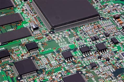
Signal integrity (SI) is a critical aspect of printed circuit board (PCB) design, ensuring that electrical signals propagate through interconnects with minimal distortion, noise, and timing errors. As modern electronic systems demand higher speeds, lower power consumption, and increased complexity, maintaining signal integrity becomes increasingly challenging. Poor signal integrity can lead to data corruption, electromagnetic interference (EMI), and system failures.
This article explores the fundamentals of PCB signal integrity analysis, including key concepts, analysis techniques, common challenges, and best practices for ensuring robust signal transmission.
2. Fundamentals of Signal Integrity
Signal integrity refers to the quality of an electrical signal as it travels from a transmitter to a receiver. Key factors affecting signal integrity include:
2.1 Transmission Line Effects
At high frequencies, PCB traces behave as transmission lines rather than simple conductors. When signal wavelengths approach trace lengths, impedance mismatches, reflections, and signal degradation become significant concerns.
2.2 Impedance Matching
Impedance mismatches between traces, connectors, and components cause signal reflections, leading to overshoot, undershoot, and ringing. Controlled impedance design (e.g., microstrip and stripline traces) helps mitigate these effects.
2.3 Crosstalk
Crosstalk occurs when electromagnetic coupling between adjacent traces induces unwanted noise. It can be categorized as:
- Capacitive Crosstalk: Due to electric field coupling.
- Inductive Crosstalk: Due to magnetic field coupling.
2.4 Power Integrity (PI) and Ground Bounce
Power delivery network (PDN) issues, such as voltage drops and ground bounce, can distort signals. Decoupling capacitors and proper power plane design help stabilize supply voltages.
2.5 Signal Attenuation and Dispersion
High-frequency signals suffer from dielectric and conductor losses, leading to attenuation and dispersion. Material selection (e.g., low-loss dielectrics) and proper trace geometry help minimize losses.
3. Signal Integrity Analysis Techniques
To ensure reliable signal transmission, engineers employ various analysis techniques:
3.1 Time-Domain Reflectometry (TDR)
TDR measures impedance variations along a transmission line by sending a fast pulse and analyzing reflections. It helps identify discontinuities, such as vias, connectors, or impedance mismatches.
3.2 Frequency-Domain Analysis
- S-Parameter Analysis: Scattering parameters (S-parameters) characterize signal behavior in the frequency domain, helping analyze insertion loss, return loss, and crosstalk.
- Eye Diagram Analysis: Eye diagrams visualize signal quality by overlaying multiple bit transitions, revealing jitter, noise, and intersymbol interference (ISI).
3.3 Electromagnetic (EM) Simulation
Full-wave EM solvers (e.g., Ansys HFSS, CST Studio) model high-frequency effects, including radiation, coupling, and dispersion, providing accurate SI predictions.
3.4 Power Integrity Analysis
Tools like Cadence Sigrity and HyperLynx analyze PDN impedance, decoupling capacitor placement, and transient noise to ensure stable power delivery.
4. Common Signal Integrity Challenges
Several challenges arise in high-speed PCB designs:
4.1 High-Speed Serial Links
Modern interfaces (PCIe, USB, DDR, HDMI) operate at multi-gigabit rates, requiring precise impedance control and minimal jitter.
4.2 Via Stub Effects
Unused via stubs act as resonant structures, causing signal reflections. Back-drilling (stub removal) mitigates this issue.
4.3 Differential Pair Routing
Differential signals (e.g., USB, Ethernet) require tight length matching and controlled skew to maintain signal balance.
4.4 EMI and Radiated Emissions
Poor SI can lead to EMI, causing compliance failures. Proper shielding, grounding, and filtering are essential.
4.5 Material Selection
High-frequency PCBs require low-loss materials (e.g., Rogers, Isola) to minimize dielectric losses.
5. Best Practices for Signal Integrity
To optimize SI in PCB designs, engineers should follow these guidelines:
5.1 Controlled Impedance Design
- Use impedance calculators to determine trace width, spacing, and dielectric thickness.
- Match trace impedance to driver/receiver specifications (e.g., 50Ω single-ended, 100Ω differential).
5.2 Minimize Crosstalk
- Increase spacing between critical traces.
- Use ground planes as shields.
- Route adjacent traces orthogonally on different layers.
5.3 Optimize Power Distribution
- Use low-inductance decoupling capacitors.
- Implement solid power and ground planes.
- Analyze PDN impedance with simulation tools.
5.4 Proper Termination Techniques
- Series termination for point-to-point links.
- Parallel termination for multi-drop buses.
- AC termination for high-speed signals.
5.5 Simulation-Driven Design
- Perform pre-layout and post-layout SI simulations.
- Validate designs with eye diagrams and TDR measurements.
6. Future Trends in Signal Integrity
As data rates continue to increase (e.g., 112G SerDes, PCIe 6.0), new challenges emerge:
- Advanced Materials: Ultra-low-loss dielectrics for mmWave applications.
- 3D Packaging: SI analysis for chiplets and interposers.
- AI-Assisted SI Optimization: Machine learning for automated SI tuning.
7. Conclusion
Signal integrity analysis is essential for ensuring reliable high-speed PCB designs. By understanding transmission line effects, utilizing simulation tools, and following best practices, engineers can mitigate signal degradation, crosstalk, and EMI. As technology advances, continuous improvements in materials, simulation techniques, and design methodologies will be crucial for maintaining robust signal integrity in next-generation electronics.


