Pcb via manufacturing
Understanding The Basics Of PCB Via Manufacturing
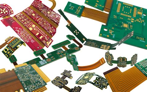
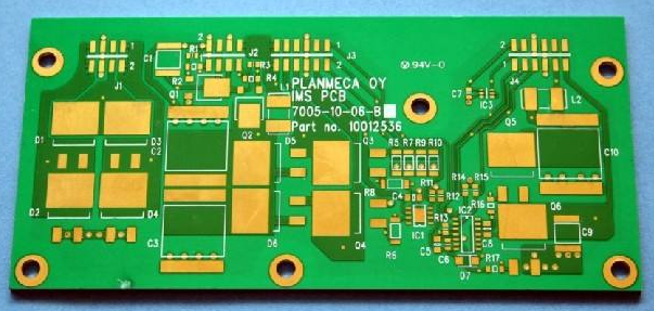
Printed Circuit Boards (PCBs) are the backbone of modern electronic devices, providing the necessary pathways for electrical signals to travel between various components.
One critical aspect of PCB design and manufacturing is the implementation of vias.
Vias are small conductive pathways that allow electrical connections between different layers of a PCB. Understanding the basics of PCB via manufacturing is essential for anyone involved in electronics design and production.
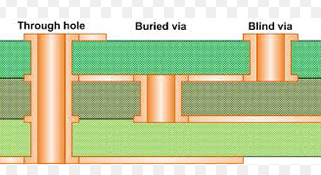
To begin with, vias are typically categorized into three main types: through-hole vias, blind vias, and buried vias.
Through-hole vias are the most common and simplest type, extending from the top layer to the bottom layer of the PCB. These vias are drilled through the entire board and then plated with a conductive material, usually copper, to establish an electrical connection. Blind vias, on the other hand, connect an outer layer to one or more inner layers but do not go through the entire board. Buried vias are located entirely within the inner layers of the PCB, connecting two or more internal layers without reaching the outer surfaces.
The manufacturing process of vias involves several critical steps, starting with drilling.
Drilling is performed using either mechanical drills or laser drills, depending on the size and precision required. Mechanical drilling is suitable for larger vias, typically those with diameters greater than 0.2 mm. Laser drilling, however, is used for microvias, which are smaller than 0.15 mm in diameter. The choice of drilling method significantly impacts the accuracy and quality of the vias.
Following the drilling process, the next step is plating.
Plating involves depositing a thin layer of conductive material, usually copper, onto the walls of the drilled holes. This is achieved through a process called electroplating, where the PCB is submerged in a copper sulfate solution, and an electric current is applied. The current causes copper ions to deposit onto the walls of the vias, forming a conductive pathway. Ensuring uniform plating is crucial, as any inconsistencies can lead to electrical failures or reduced reliability of the PCB.
After plating, the vias undergo a series of inspections and tests to verify their integrity and functionality.
These inspections include visual checks, X-ray analysis, and electrical testing. Visual inspections help identify any obvious defects, such as incomplete plating or misalignment. X-ray analysis provides a more detailed view of the internal structure of the vias, ensuring that the plating is uniform and free of voids. Electrical testing involves measuring the resistance of the vias to ensure they provide a reliable conductive path.
In addition to these standard processes, advanced techniques such as via-in-pad and via filling are also employed in modern PCB manufacturing.
Via-in-pad involves placing vias directly beneath surface-mounted components, which helps save space and improve signal integrity. Via filling, on the other hand, involves filling the vias with conductive or non-conductive materials to enhance mechanical strength and thermal performance.
Understanding the basics of PCB via manufacturing is crucial for designing reliable and efficient electronic devices. The choice of via type, drilling method, and plating process all play a significant role in the overall performance and durability of the PCB. By mastering these fundamental aspects, designers and manufacturers can ensure the production of high-quality PCBs that meet the stringent demands of modern electronics.
Advanced Techniques In PCB Via Fabrication
Printed Circuit Boards (PCBs) are the backbone of modern electronic devices, and the vias within these boards play a crucial role in their functionality. Vias, which are small conductive pathways that connect different layers of a PCB, are essential for the transmission of electrical signals. As electronic devices become more complex and miniaturized, advanced techniques in PCB via fabrication have become increasingly important to ensure reliability and performance.
One of the most significant advancements in PCB via manufacturing is the development of microvias.
Unlike traditional vias, which are relatively large and can occupy substantial space on a PCB, microvias are much smaller and can be placed more densely. This allows for more complex and compact designs, which is particularly beneficial for high-density interconnect (HDI) PCBs. The fabrication of microvias typically involves laser drilling, a technique that offers high precision and can create vias with diameters as small as 50 micrometers. This precision is crucial for maintaining the integrity of the electrical connections and ensuring the overall performance of the PCB.
In addition to microvias, another advanced technique in PCB via fabrication is the use of buried and blind vias.
Traditional through-hole vias extend from the top to the bottom layer of a PCB, which can be inefficient for multi-layer boards. Buried vias, on the other hand, connect internal layers without reaching the outer surfaces, while blind vias connect an outer layer to one or more inner layers without passing through the entire board. These types of vias help to optimize the use of space within the PCB, allowing for more intricate designs and reducing the overall size of the board.
Furthermore, the implementation of via-in-pad technology has revolutionized PCB design and manufacturing.
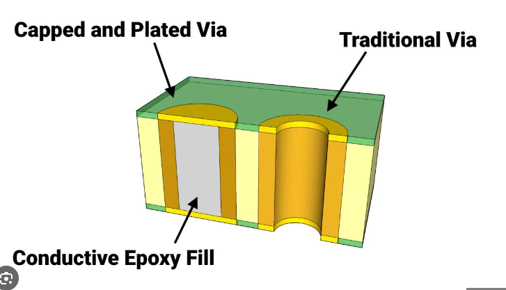
Via-in-pad involves placing vias directly beneath surface-mounted components, which helps to minimize signal path lengths and improve electrical performance. This technique is particularly useful for high-frequency applications where signal integrity is paramount. However, via-in-pad fabrication requires meticulous attention to detail, as any imperfections can lead to issues such as solder voids or component misalignment. Advanced plating and filling techniques, such as copper filling or conductive epoxy, are often employed to ensure the reliability of via-in-pad structures.
Another noteworthy advancement in PCB via fabrication is the use of advanced materials and coatings.
Traditional vias are typically made from copper, but the introduction of alternative materials such as silver or gold can enhance conductivity and reduce resistance. Additionally, the application of specialized coatings can improve the thermal and mechanical properties of vias, making them more resilient to environmental stresses. For instance, the use of nickel-gold plating can provide excellent corrosion resistance and ensure long-term reliability, which is particularly important for PCBs used in harsh environments.
Moreover, the integration of advanced inspection and testing methods has significantly improved the quality control of PCB vias.
Techniques such as X-ray inspection and automated optical inspection (AOI) allow for the detection of defects that may not be visible to the naked eye. These methods ensure that any issues are identified and addressed early in the manufacturing process, thereby reducing the risk of failures in the final product.
In conclusion, the advancements in PCB via fabrication have been instrumental in meeting the demands of modern electronic devices. From the development of microvias and via-in-pad technology to the use of advanced materials and inspection methods, these techniques have enabled the creation of more compact, reliable, and high-performing PCBs. As technology continues to evolve, it is likely that further innovations in via fabrication will emerge, driving the next generation of electronic devices.

Common Challenges In PCB Via Production And How To Overcome Them
Printed Circuit Board (PCB) via manufacturing is a critical process in the electronics industry, enabling the interconnection of different layers within a PCB. However, this process is fraught with challenges that can impact the performance and reliability of the final product. Understanding these common challenges and implementing strategies to overcome them is essential for ensuring high-quality PCB production.
One of the primary challenges in PCB via manufacturing is the accurate drilling of vias.
Vias, which are small holes that allow electrical connections between different layers of a PCB, must be drilled with precision. Any deviation in the drilling process can lead to misalignment, which can cause electrical failures or short circuits. To mitigate this issue, manufacturers often employ advanced drilling machines equipped with high-precision tools and automated systems. These machines can achieve the necessary accuracy and consistency, reducing the risk of misalignment.
Another significant challenge is the plating of vias.
The plating process involves depositing a thin layer of conductive material, usually copper, inside the drilled holes to establish electrical connections. Inadequate plating can result in poor conductivity and increased resistance, which can degrade the performance of the PCB. To address this, manufacturers use electroplating techniques that ensure uniform deposition of the conductive material. Additionally, regular monitoring and quality control checks are essential to detect and rectify any plating defects early in the production process.
Thermal management is also a critical concern in PCB via manufacturing.
Vias can act as thermal conduits, transferring heat between different layers of the PCB. If not properly managed, this heat transfer can lead to overheating and potential damage to the components. To overcome this challenge, manufacturers often use thermal vias, which are specifically designed to dissipate heat more effectively. These vias are typically filled with thermally conductive materials that enhance heat transfer away from critical components, thereby improving the overall thermal performance of the PCB.
Contamination is another issue that can compromise the integrity of PCB vias.
During the manufacturing process, contaminants such as dust, oils, and residues can accumulate inside the vias, leading to poor electrical connections and potential failures. To prevent contamination, manufacturers implement stringent cleaning protocols and use cleanroom environments to minimize the presence of foreign particles. Additionally, advanced inspection techniques, such as X-ray imaging, are employed to detect and address any contamination issues before the final assembly.
The miniaturization of electronic devices has also introduced new challenges in PCB via manufacturing.
As devices become smaller and more complex, the demand for smaller vias with higher density increases. This miniaturization requires advanced manufacturing techniques and materials that can support the reduced sizes without compromising performance. Laser drilling, for instance, is a technique that allows for the creation of smaller and more precise vias, meeting the demands of modern electronic devices.
In conclusion, PCB via manufacturing is a complex process that involves several challenges, including accurate drilling, effective plating, thermal management, contamination control, and miniaturization. By employing advanced technologies, stringent quality control measures, and innovative manufacturing techniques, these challenges can be effectively addressed. Ensuring the reliability and performance of PCB vias is crucial for the overall success of electronic devices, making it imperative for manufacturers to continuously improve their processes and stay abreast of technological advancements in the field.
Innovations In PCB Via Technology For Enhanced Performance
Printed Circuit Boards (PCBs) are the backbone of modern electronic devices, and their performance is critically dependent on the quality and efficiency of their vias. Vias, the small holes that allow electrical connections between different layers of a PCB, have seen significant innovations in recent years.
These advancements are driven by the increasing demand for miniaturization, higher performance, and greater reliability in electronic devices. As a result, manufacturers are continually exploring new materials, techniques, and designs to enhance the functionality and efficiency of PCB vias.
One of the most notable innovations in PCB via technology is the development of microvias.
Unlike traditional vias, which are relatively large and can occupy significant space on a PCB, microvias are much smaller and can be used to create more compact and densely packed circuit designs. This is particularly beneficial for applications in smartphones, tablets, and other portable devices where space is at a premium. Microvias are typically created using laser drilling, which allows for precise control over the size and placement of the vias, resulting in improved electrical performance and reduced signal loss.
In addition to microvias, another significant advancement is the use of via-in-pad technology.
This technique involves placing the via directly within the pad of a surface-mounted component, rather than in the surrounding area. This approach not only saves space but also enhances the thermal and electrical performance of the PCB. By reducing the distance that signals need to travel, via-in-pad technology minimizes signal degradation and improves overall device performance. Furthermore, this method can help to reduce the number of layers required in a PCB, leading to cost savings and increased manufacturing efficiency.
The materials used in via construction have also seen considerable innovation.
Traditionally, vias have been made using copper, which offers excellent electrical conductivity. However, as the demand for higher performance and reliability has grown, manufacturers have begun to explore alternative materials. For instance, the use of advanced copper alloys and other conductive materials can provide better thermal management and improved mechanical strength. Additionally, the incorporation of conductive polymers and nanomaterials has shown promise in enhancing the performance of PCB vias, particularly in high-frequency applications.
Another area of innovation is the development of advanced via filling techniques.
In the past, vias were often left hollow, which could lead to issues with reliability and performance. Today, manufacturers are increasingly using via filling methods, such as copper filling or conductive epoxy filling, to create solid vias. These filled vias offer several advantages, including improved thermal conductivity, enhanced mechanical stability, and reduced risk of voids or defects. This is particularly important for high-density interconnect (HDI) PCBs, where the reliability of each via is critical to the overall performance of the device.
Moreover, the advent of advanced simulation and modeling tools has revolutionized the design and optimization of PCB vias.
These tools allow engineers to accurately predict the electrical, thermal, and mechanical behavior of vias under various conditions, enabling them to make informed decisions about via placement, size, and materials. This has led to the development of more robust and efficient PCB designs, capable of meeting the stringent demands of modern electronic applications.
In conclusion, the innovations in PCB via technology have significantly enhanced the performance and reliability of electronic devices. From the development of microvias and via-in-pad technology to the use of advanced materials and filling techniques, these advancements are driving the evolution of PCB manufacturing. As the demand for smaller, faster, and more reliable electronic devices continues to grow, it is likely that we will see even more groundbreaking developments in PCB via technology in the coming years.