Printed Circuit Board Assembly (PCBA): A Comprehensive Guide
Introduction to PCBA
Printed Circuit Board Assembly (PCBA) is a critical process in electronics manufacturing that involves mounting and soldering electronic components onto a printed circuit board (PCB). The PCBA process transforms a bare PCB into a functional electronic device, forming the backbone of modern electronics, from consumer gadgets to industrial machinery.
This article explores the PCBA process, key technologies, challenges, and future trends in the industry.
1. The PCBA Process: Step-by-Step
The PCBA process consists of several stages, each requiring precision and quality control to ensure reliable performance.
1.1 PCB Fabrication
Before assembly, the PCB itself must be manufactured. The fabrication process includes:
- Design and Layout: Using CAD software to design the circuit schematic and PCB layout.
- Substrate Preparation: Choosing materials like FR-4 (fiberglass) or flexible substrates.
- Copper Etching: Applying copper layers and etching away excess to form conductive traces.
- Drilling and Plating: Creating vias and through-holes for component leads.
- Solder Mask and Silkscreen: Adding protective layers and component labels.
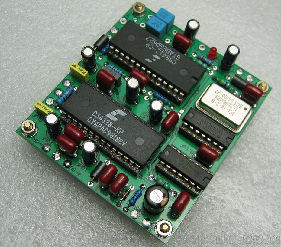
1.2 Component Placement
Once the PCB is ready, components are placed using two primary methods:
- Surface Mount Technology (SMT): Automated pick-and-place machines position tiny components (resistors, capacitors, ICs) onto pads.
- Through-Hole Technology (THT): Larger components (connectors, transformers) are inserted into drilled holes and soldered manually or via wave soldering.
1.3 Soldering
Soldering secures components to the PCB:
- Reflow Soldering (for SMT): The board passes through an oven, melting solder paste to form connections.
- Wave Soldering (for THT): The PCB moves over a wave of molten solder, bonding through-hole leads.
- Selective Soldering: Used for mixed SMT/THT boards where only specific areas need soldering.
1.4 Inspection and Testing
Quality assurance is crucial:
- Automated Optical Inspection (AOI): Cameras scan for misaligned or missing components.
- X-ray Inspection: Detects hidden defects like solder voids in BGA packages.
- In-Circuit Testing (ICT): Electrical tests verify connectivity and functionality.
- Functional Testing: The assembled board is tested under real operating conditions.
1.5 Final Assembly
The PCBA may undergo additional steps:
- Conformal Coating: Protects against moisture, dust, and corrosion.
- Enclosure Integration: Mounting the PCB into a housing with connectors and interfaces.
2. Key Technologies in PCBA
2.1 Surface Mount Technology (SMT)
SMT dominates modern PCBA due to:
- Miniaturization: Supports smaller, high-density components.
- Speed and Efficiency: High-speed pick-and-place machines enable mass production.
- Cost-Effectiveness: Reduced material waste compared to THT.
2.2 Through-Hole Technology (THT)
Though declining, THT remains essential for:
- High-Power Components: Handles larger, robust parts.
- Mechanical Stability: Stronger bonds for components under stress.
2.3 Mixed Technology Assembly
Many PCBAs combine SMT and THT, requiring hybrid assembly lines.
2.4 Advanced Soldering Techniques
- Vapor Phase Soldering: Uses heated vapor for uniform temperature distribution.
- Laser Soldering: Precise soldering for sensitive components.
2.5 Industry 4.0 and Smart Manufacturing
- Automation: Robotics and AI optimize assembly lines.
- IoT Integration: Real-time monitoring of production defects.
- Digital Twins: Simulating PCBA processes before physical production.
3. Challenges in PCBA Manufacturing
Despite advancements, PCBA faces several challenges:
3.1 Component Shortages
Global supply chain disruptions (e.g., semiconductor shortages) delay production.
3.2 Miniaturization and High-Density Designs
- Fine-Pitch Components: Difficult to place and solder accurately.
- Thermal Management: Heat dissipation in compact designs.
3.3 Soldering Defects
Common issues include:
- Bridging: Solder shorts between adjacent pins.
- Tombstoning: Components lifting due to uneven heating.
- Cold Joints: Weak solder connections from insufficient heat.
3.4 Environmental Regulations
- RoHS Compliance: Restricts hazardous materials (lead, mercury).
- Waste Management: Proper disposal of solder and chemicals.
4. Future Trends in PCBA
4.1 Flexible and Rigid-Flex PCBs
- Growing demand for bendable electronics in wearables and medical devices.
4.2 3D Printed Electronics
- Additive manufacturing enables rapid prototyping of complex PCB designs.
4.3 AI and Machine Learning
- Predictive maintenance for assembly machines.
- AI-driven defect detection in real-time.
4.4 Green Manufacturing
- Lead-free soldering and biodegradable substrates.
- Energy-efficient production techniques.
4.5 High-Speed and High-Frequency PCBs
- 5G and IoT devices require advanced materials for signal integrity.
Conclusion
PCBA is a sophisticated and evolving field that plays a vital role in electronics manufacturing. From automated SMT assembly to AI-driven quality control, advancements continue to enhance efficiency and reliability. However, challenges like component shortages and environmental regulations require ongoing innovation.
As technology progresses, trends like flexible PCBs, 3D printing, and smart manufacturing will shape the future of PCBA, enabling smaller, faster, and more sustainable electronic devices.


