Qualified engineers must understand the electromagnetic compatibility issues of PCB circuit design
Qualified engineers must understand the electromagnetic compatibility issues of PCB circuit design
1.General concept of electromagnetic compatibility
The fundamental reason for considering electromagnetic compatibility lies in the existence of electromagnetic interference. Electromagnetic interference (EMI) is the process by which destructive electromagnetic energy is transmitted from one electronic device to another through radiation or conduction. Generally speaking, EMI refers specifically to radio frequency signals (RF), but electromagnetic interference can occur in all frequency ranges.
Electromagnetic compatibility (EMC) refers to the ability of electrical and electronic systems, equipment and devices to operate at the designed level or performance within the specified safety limits in a set electromagnetic environment without being damaged or unacceptably deteriorating due to electromagnetic interference. The electromagnetic environment here refers to the sum of all electromagnetic phenomena present in a given place. This shows that electromagnetic compatibility means that electronic products should have the ability to suppress external electromagnetic interference on the one hand; on the other hand, the electromagnetic interference generated by the electronic product should be below the limit and should not affect the normal operation of other electronic devices in the same electromagnetic environment.
Today’s electronic products have changed from analog design to digital design.
With the development of digital logic devices, issues related to EMI and EMC have begun to become the focus of products and have received great attention from designers and users. The FCC of the United States announced the radiation standards for personal computers and similar equipment in the mid-to-late 1970s, and the European Community proposed mandatory requirements for radiation and anti-interference in its 89/336/EEC electromagnetic compatibility guidance document. my country has also successively formulated national standards and national military standards for electromagnetic compatibility, such as “Electromagnetic Compatibility Terms” (GB/T4365-1995), “Electromagnetic Interference and Electromagnetic Compatibility Terms” (GJB72-85), “Radio Interference and Immunity Measurement Equipment Specification” (GB/T6113-1995), “Measurement Methods and Allowable Values of Radio Interference Characteristics of Power Tools, Household Appliances and Similar Appliances” (GB4343-84). These electromagnetic compatibility specifications have greatly promoted electronic design technology and improved the reliability and applicability of electronic products.
2.The Importance of EMC in PCB Design
As the sensitivity of electronic equipment becomes higher and higher, and the ability to receive weak signals becomes stronger and stronger, the frequency band of electronic products becomes wider and wider, the size becomes smaller and smaller, and the anti-interference ability of electronic equipment becomes stronger and stronger.
The electromagnetic waves generated by some electrical and electronic equipment when they are working can easily cause electromagnetic interference to other electrical and electronic equipment around them, causing failures or affecting signal transmission. In addition, excessive electromagnetic interference will cause electromagnetic pollution, endanger people’s health and damage the ecological environment.
If various electrical equipment in a system can work normally without electromagnetic interference with each other, causing performance changes and equipment damage, people say that the electrical equipment in this system is compatible with each other. However, with the diversification of equipment functions, complexity of structure, increase in power and increase in frequency, and their sensitivity is also getting higher and higher, this state of mutual compatibility is becoming more and more difficult to obtain. In order to make the system electromagnetically compatible, it must be based on the electromagnetic environment of the system, requiring each electrical equipment not to generate electromagnetic emissions exceeding a certain limit, and at the same time requiring it to have a certain anti-interference ability. Only by making these two constraints and improvements on each device can the system be fully compatible.
It is generally believed that there are two ways to transmit electromagnetic interference: one is conduction; the other is radiation. In actual engineering, interference between two devices usually involves coupling in many ways. It is precisely because of the simultaneous existence of multiple coupling paths, repeated crosstalk, and the joint interference that electromagnetic interference becomes difficult to control.
Common electromagnetic interference mainly includes the following types:
(1) Radio frequency interference. Due to the surge in existing radio transmitters, radio frequency interference poses a great threat to electronic systems. Cellular phones, handheld radios, radio remote control units, pagers and other similar devices are now very common. It does not take a lot of power to cause harmful interference. Typical failures occur in the RF field strength range of 1 to 10V/m. In Europe, North America and many Asian countries, avoiding radio frequency interference from damaging other equipment has become a legally mandatory requirement for all products.
(2) Electrostatic discharge (ESD). Modern chip technology has made great progress, and components have become very dense on a very small geometric size (0.18um). These high-speed, millions of transistor microprocessors are highly sensitive and can be easily damaged by external electrostatic discharge. Discharge can be caused by direct or radiated means. Direct contact discharge generally causes permanent damage to the device. Electrostatic discharge caused by radiation may cause equipment disorder and malfunction.
(3) Power interference. As more and more electronic devices are connected to the power main grid, some potential interference will appear in the system. These interferences include power line interference, electrical fast transients, surges, voltage changes, lightning transients and power line harmonics. For high-frequency switching power supplies, these interferences become very significant.
(4) Self-compatibility. The digital part or circuit of a system may interfere with analog devices, generate crosstalk between wires, or a motor can cause disorder in digital circuits.
In addition, an electronic product that can work normally at low frequencies will encounter some problems that do not exist at low frequencies when the frequency increases. For example, reflection, crosstalk, ground bounce, high-frequency noise, etc.
An electronic product that does not meet EMC specifications is not a qualified electronic design. In addition to meeting the functional requirements of the market, the design product must also adopt appropriate design techniques to prevent or eliminate the impact of EMI.
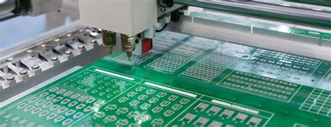
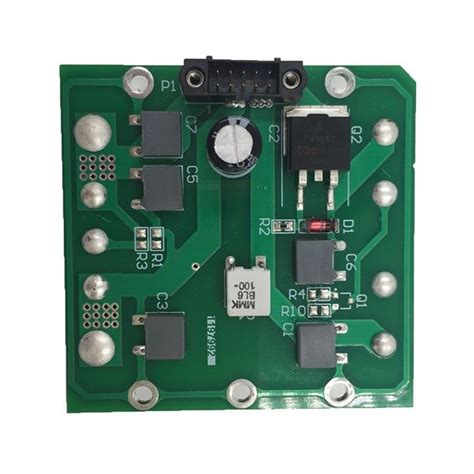
3.EMC considerations for PCB design
There are usually two ways to solve EMI problems in high-speed PCB (Printed Circuit Board) design: one is to suppress the impact of EMI, and the other is to shield the impact of EMI. There are many different manifestations of these two methods, especially the shielding system, which minimizes the possibility of EMI affecting electronic products.
Radio frequency (RF) energy is generated by switching currents in printed circuit boards (PCBs), which are byproducts of digital components. Every change in logic state in a power distribution system will generate a momentary surge. In most cases, these changes in logic state will not generate enough ground noise voltage to cause any functional impact, but when the edge rate (rise time and fall time) of a component becomes quite fast, it will generate enough RF energy to affect the normal operation of other electronic components.
3.1 Causes of electromagnetic interference on PCBs
Improper practices usually cause EMI on PCBs that exceeds the specification. Combined with the characteristics of high-frequency signals, the main aspects related to PCB-level EMI include the following:
(1) Improper use of packaging measures. For example, a device that should be packaged in metal is packaged in plastic.
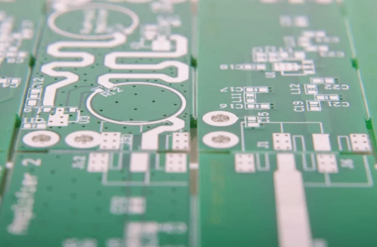
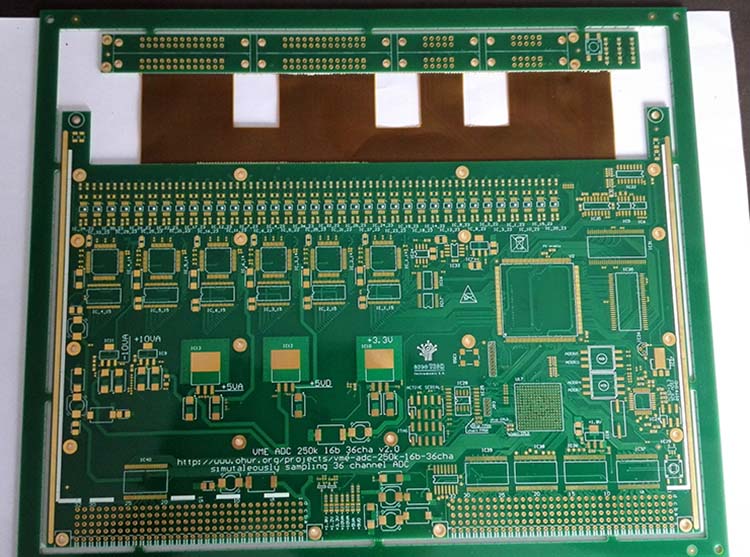
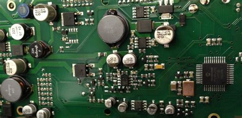
(2) Poor PCB design, poor finishing quality, and poor grounding of cables and connectors.
(3) Improper or even incorrect PCB layout.
Including improper setting of clock and periodic signal routing; improper layering arrangement of PCB and signal wiring layer setting; improper selection of high-frequency RF energy distribution components; insufficient consideration of common mode and differential mode filtering; ground loop causes RF and ground bounce; insufficient bypass and decoupling, etc.
To achieve system-level EMI suppression, some appropriate methods are usually required: this mainly includes shielding, padding, grounding, filtering, decoupling, proper wiring, circuit impedance control, etc.
3.2 Shielding design for electromagnetic compatibility
Today’s electronics industry has increasingly noticed the need for SE/EMC (Shielding Effectiveness, SE, isolation room shielding effectiveness), and with the use of more electronic components, electromagnetic compatibility has also received more attention. Electromagnetic shielding is a method of controlling the induction and radiation propagation of electromagnetic interference from one area to another based on the principle of metal isolation.
Usually there are two types: one is electrostatic shielding, which is mainly used to prevent the influence of electrostatic fields and constant magnetic fields; the other is electromagnetic shielding, which is mainly used to prevent the influence of alternating electric fields, alternating magnetic fields and alternating electromagnetic fields.
EMI shielding can make the product meet EMC specifications simply and effectively.
When the frequency is below 10MHz, electromagnetic waves are mostly in the form of conduction, while higher frequency electromagnetic waves are mostly in the form of radiation. When designing, new materials such as single-layer solid shielding materials, multi-layer solid shielding materials, double shielding or double shielding or more can be used for EMI shielding.
For low-frequency electromagnetic interference, a thick shielding layer is required.
The most suitable material is a material with high magnetic permeability or a magnetic material, such as nickel-copper alloy, to obtain the maximum electromagnetic absorption loss, while for high-frequency electromagnetic waves, metal shielding materials can be used.
In actual EMI shielding, the effectiveness of electromagnetic shielding depends largely on the physical structure of the chassis, that is, the continuity of conductivity. The seams and openings on the chassis are sources of electromagnetic wave leakage. Moreover, the cables passing through the chassis are also the main reason for the decline in shielding effectiveness.
The electromagnetic leakage of the opening on the chassis is related to the shape of the opening, the characteristics of the radiation source, and the distance from the radiation source to the opening. The shielding effectiveness can be improved by properly designing the opening size and the distance from the radiation source to the opening. The usual way to solve the electromagnetic leakage of the chassis gap is to use an electromagnetic sealing gasket at the gap. Electromagnetic sealing gasket is a conductive elastic material that can maintain the continuity of conductivity at the gap.

Common electromagnetic sealing gaskets include: conductive rubber (conductive particles are added to the rubber so that the composite material has both the elasticity of rubber and the conductivity of metal.), double conductive rubber (it does not add conductive particles to all parts of the rubber.
The benefit obtained in this way is that it can maximize the elasticity of the rubber and ensure the conductivity), metal braided mesh sleeve (metal braided mesh sleeve with rubber as the core), spiral tube gasket (spiral tube rolled with stainless steel, beryllium copper or tinned beryllium copper), etc. In addition, when the ventilation volume is required to be relatively high, a cut-off waveguide ventilation plate must be used. This plate is equivalent to a high-pass filter. It does not attenuate electromagnetic waves above a certain frequency, but it greatly attenuates electromagnetic waves below this frequency. Reasonable application of this characteristic of the cut-off waveguide can well shield EMI interference.
3.3 Reasonable PCB design for electromagnetic compatibility
With the large-scale increase in system design complexity and integration, electronic system designers are engaged in circuit design above 100MHZ, and the operating frequency of the bus has reached or exceeded 50MHZ, and some even exceed 100MHZ. When the system operates at 50MHz, transmission line effects and signal integrity problems will occur; and when the system clock reaches 120MHz, unless high-speed circuit design knowledge is used, the PCB designed based on traditional methods will not work. Therefore, high-speed circuit design technology has become a design method that electronic system designers must adopt. Only by using the design technology of high-speed circuit designers can the controllability of the design process be achieved.
It is generally believed that if the frequency of a digital logic circuit reaches or exceeds 45MHZ~50MHZ, and the circuit operating above this frequency has accounted for a certain proportion of the entire electronic system (for example, 1/3), it is called a high-speed circuit. In fact, the harmonic frequency of the signal edge is higher than the frequency of the signal itself. It is the rising and falling edges of the signal that change rapidly (or the jump of the signal) that trigger the unexpected result of signal transmission. To achieve high-frequency PCB design that meets EMC standards, the following technologies are usually required: bypass and decoupling, ground control, transmission line control, and routing terminal matching.
(1) Bypass and decoupling
Decoupling refers to the removal of RF energy that enters the power distribution network from high-frequency devices when the device switches, while bypassing is the transfer of unwanted common-mode RF energy from components or cables.
All capacitors are composed of LCR circuits, where L is the inductance, which is related to the length of the wire, R is the resistance in the wire, and C is the capacitance. At a certain frequency, this LC series combination will resonate. In the resonant state, the LCR circuit will have very small impedance and effective RF bypass. When the frequency is higher than the self-resonance of the capacitor, the capacitor gradually becomes an inductive impedance, and the bypass or decoupling effect decreases. Therefore, the effect of the capacitor in achieving bypass and decoupling is affected by the lead length, the routing between the capacitor and the device, the dielectric filler, etc. An ideal decoupling capacitor can also provide all the current required when the logic device switches state. In fact, the impedance between the power supply and the ground layer determines how much current the capacitor can provide.
When selecting bypass and decoupling capacitors, the self-resonant frequency of the required capacitor can be calculated by the logic series and the clock speed used, and the capacitance value can be selected according to the frequency and the capacitive reactance in the circuit. When selecting the package size, try to choose capacitors with lower lead inductance, which are usually manifested as SMT (Surface Mount Technology) capacitors, rather than through-hole capacitors (such as DIP packaged capacitors). In addition, in product design, parallel decoupling capacitors are often used to provide a larger operating frequency band and reduce ground imbalance. In a parallel capacitor system, when it is higher than the self-resonant frequency, the large capacitor exhibits inductive impedance and increases with the frequency; while the small capacitor exhibits capacitive impedance and decreases with the frequency, and at this time the impedance of the entire capacitor circuit is smaller than the impedance of a single capacitor.