Quality Assurance in PCB Manufacturing: Ensuring Design Specifications are Met
Introduction
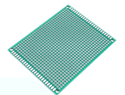
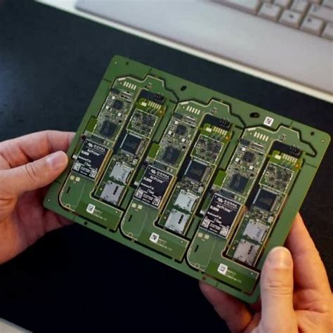
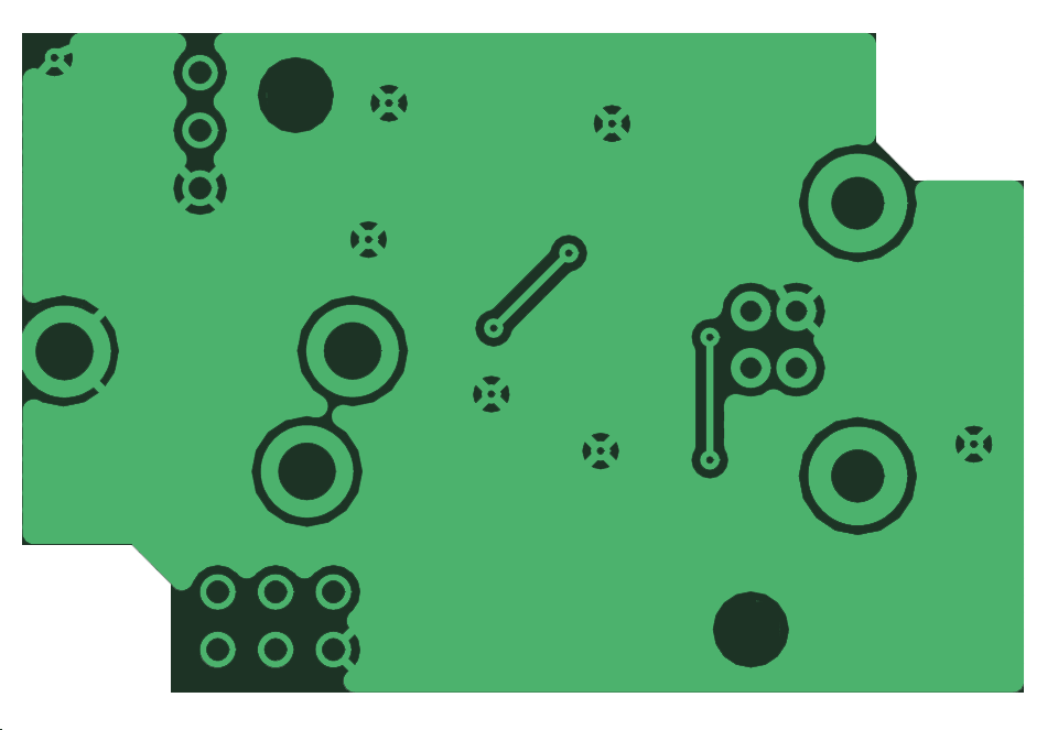
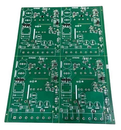
Printed Circuit Boards (PCBs) are the backbone of modern electronics, serving as the foundation for electrical connections in devices ranging from smartphones to industrial machinery. Ensuring that PCBs meet design and manufacturing specifications is critical to their performance, reliability, and longevity. Manufacturers employ a variety of inspection and testing techniques to verify that PCBs comply with design requirements before they leave the factory.
This article explores the key quality control (QC) processes used in PCB manufacturing, including visual inspections, automated optical inspections (AOI), electrical testing, and functional validation. By understanding these methods, designers and manufacturers can ensure that their PCBs meet industry standards and perform as intended in real-world applications.
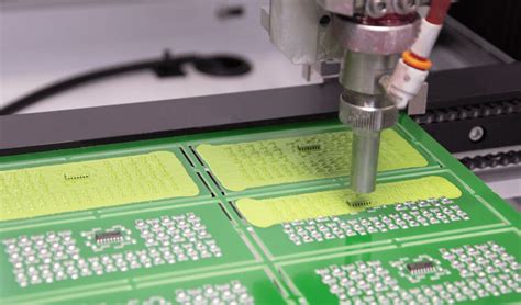
1. Visual Inspection (Manual and Automated)
The first step in PCB quality assurance is visual inspection, which can be performed manually or using automated systems.
1.1 Manual Visual Inspection (MVI)
Trained inspectors examine PCBs under magnification to identify defects such as:
- Solder bridges (unintended connections between pads)
- Insufficient or excessive solder
- Misaligned components
- Scratches or physical damage
- Incorrect component placement
While MVI is useful for small-batch production, it is time-consuming and prone to human error, making it less efficient for high-volume manufacturing.
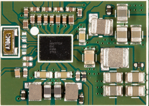
1.2 Automated Optical Inspection (AOI)
AOI systems use high-resolution cameras and machine vision algorithms to scan PCBs for defects. Key advantages include:
- High-speed inspection (suitable for mass production)
- Detection of microscopic defects (e.g., lifted pads, missing components)
- Consistency and repeatability (reduces human error)
AOI is particularly effective after solder paste application, component placement, and reflow soldering stages.
2. Electrical Testing
Electrical testing ensures that PCB circuits function as intended without short circuits or open connections.
2.1 Continuity Testing (Flying Probe Test)
- A flying probe tester checks for open circuits (broken traces) and short circuits (unwanted connections).
- It moves probes across test points to verify electrical connectivity.
- Ideal for low-volume or prototype PCBs due to its flexibility.
2.2 In-Circuit Testing (ICT)
- ICT uses a bed-of-nails fixture to make contact with test points across the PCB.
- It verifies component values (resistance, capacitance, etc.) and detects wrong or missing components.
- Best suited for high-volume production where test fixtures can be reused.
2.3 Boundary Scan Testing (JTAG)
- Used for complex digital circuits (e.g., microcontrollers, FPGAs).
- Tests interconnections between integrated circuits (ICs) without physical probes.
- Helps diagnose faults in Ball Grid Array (BGA) and other high-density components.
3. Functional Testing (FCT)
Functional testing validates that the PCB performs as expected in real-world conditions.
3.1 Power-On Testing
- The PCB is powered up to verify voltage levels, signal integrity, and basic functionality.
- Checks for overheating, unstable power delivery, or malfunctioning components.
3.2 Signal Integrity Testing
- High-speed PCBs (e.g., RF, DDR memory interfaces) require impedance matching and signal quality checks.
- Techniques include Time-Domain Reflectometry (TDR) and Eye Diagram Analysis.
3.3 Environmental Stress Testing
- PCBs may undergo thermal cycling, humidity exposure, and vibration tests to ensure reliability.
- Helps identify weak solder joints or material degradation.
4. X-Ray Inspection (AXI) for Hidden Defects
Some PCB defects, such as voids in solder joints or misaligned BGA connections, are not visible to optical inspection. Automated X-ray Inspection (AXI) provides:
- 3D imaging of internal structures (e.g., solder ball integrity in BGAs).
- Detection of hidden cracks or voids in plated through-holes (PTHs).
- Non-destructive testing (preserves the PCB for further use).
AXI is essential for high-reliability applications (medical, aerospace, automotive).
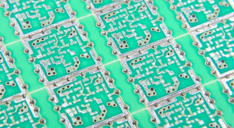
5. Design Rule Checking (DRC) and Manufacturing Feedback
Before PCBs are fabricated, manufacturers run Design Rule Checks (DRC) to ensure the design meets manufacturing capabilities. Post-production, feedback loops help improve future designs by identifying:
- Common failure points (e.g., thin traces prone to breaking).
- Soldering issues (e.g., thermal relief problems).
- Optimization opportunities (e.g., better component placement).
Conclusion
Ensuring that PCBs meet design specifications requires a multi-layered approach involving visual inspections, electrical tests, functional validation, and advanced imaging techniques. By implementing rigorous quality control measures, manufacturers can deliver reliable, high-performance PCBs that meet industry standards and customer expectations.
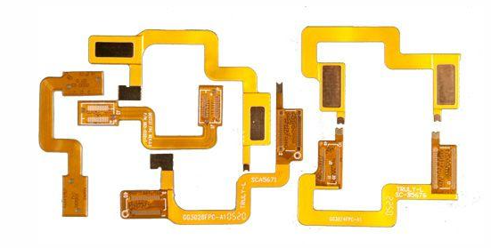
As PCB technology evolves—with trends like high-density interconnects (HDI), flexible PCBs, and IoT miniaturization—quality assurance methods must also advance to detect increasingly subtle defects. Collaboration between designers and manufacturers is key to producing defect-free PCBs that power the next generation of electronic devices.