Rigid-Flex Circuit Design Considerations for Wearable Temperature Sensor Applications
Abstract
This article provides general design guidelines for developing rigid-flex circuit boards for measuring core body temperature (CBT) sensor products for a variety of high-precision (±0.1°C) temperature sensing applications.
The recommendations in this article were used by Texas A&M University and Analog Devices in their joint development of a CBT sensor product. This CBT device uses four MAX30208 temperature sensors to measure heat flux to accurately estimate a subject’s CBT. 1,2
Introduction
This article is intended to help designers identify and address several potential issues when designing high-precision (±0.1°C) temperature sensing circuits. This guide uses a recent CBT design as an example to address the thermal, electrical, and mechanical aspects and to make appropriate trade-offs in these areas. These considerations will help designers:
- Understand how to identify design challenges, trade-offs, and techniques associated with developing high-precision CBT sensing devices.
- Understand how to design a reliable rigid-flex printed circuit board for remote patient monitoring applications.
- Apply the design guidelines to heat flux and mechanical structures.
- Rigid-flex PCB manufacturing.
CBT device design overview
As a flexible wearable thermal sensing device, the CBT patch can accurately estimate human CBT (Figure 1a). Figure 1b shows the main components of the thermal sensing device, which consists of four temperature sensors (MAX30208). These sensors are separated by materials of different thermal conductivities to accurately quantify CBT. These temperature sensors have an accuracy of 0.1°C and a supply voltage of 1.8V, which supports low-power operation. Among them, one temperature sensor is located in the center of the PCB, two temperature sensors are located in the middle and edge of the PCB, and the fourth sensor is located at the tip of the flexible touch patch, which is folded toward the center of the PCB. (Figure 1c).
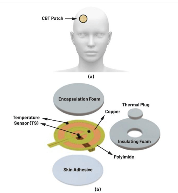
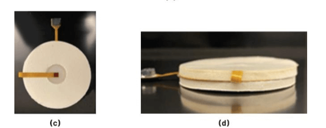
Figure 1. CBT device design. (a) The wearable thermal sensing device is placed on the forehead to estimate human CBT; (b) 3D exploded view of the CBT patch; (c) The human tissue side of the flexible CBT patch; (d) Side view of the flexible CBT patch.
The CBT patch is used to monitor patient temperature in preoperative, intraoperative, and postoperative environments. Typical ambient temperatures for this type of environment range from 20°C to 24°C, with a maximum air thermal conductivity of 5 W/m2/K. Normal range for forehead core body temperature is 36°C to 38°C. Conditions below 36°C are called hypothermia, and conditions above 38°C are called hyperthermia. Both conditions are serious, so core body temperature needs to be monitored at all stages of surgery.
Layout Design Considerations for Heat Flow
The CBT patch product is designed to measure heat flow perpendicular to the surface of human tissue using two MAX30208 temperature sensors. As shown in Figure 2, TS is the MAX30208 temperature sensor. The other two temperature sensors shown in Figure 1 help calculate lateral heat losses. Combining the temperature sensor data with the thermal model of the conductive plug and insulating housing can accurately estimate the CBT of the human forehead.
To achieve this goal, the rigid-flex PCB with temperature sensing circuit needs to:
- Integrate a high-precision temperature sensor.
- The power consumption of the temperature sensor should be low enough not to adversely affect the associated thermal system.
- Have sufficiently thick PCB traces for signal transmission.
- The size of the signal trace should be sufficient to reduce the heat flow from (or to) the MAX30208 temperature sensor to avoid adversely affecting the thermal system.
- The size of the signal trace should minimize the heat radiation (i.e., I2R losses) from the PCB trace to the conductive plug area.
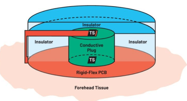
Figure 2. The main temperature sensing paths (not drawn to scale).
By using appropriate thermally conductive/insulating materials and designing their physical structure, it is possible to accurately estimate the CBT of the forehead. In combination with a high-precision, low-power temperature sensor such as the MAX30208, a successful product design can be achieved. However, electrical connections such as PCB traces of electronic devices also conduct heat – this is undesirable!
Figure 3 shows the relevant heat flow paths. We want to design the thermal resistance of the PCB trace to be much larger than that of the conductive plug to ensure that the error caused by these additional heat losses (or gains) is negligible.
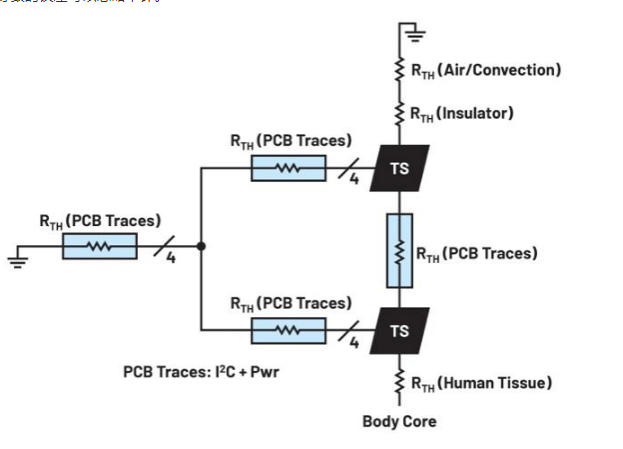
Figure 3. Simplified thermal schematic showing the main heat flow paths.
Since both heat and electricity are transferred through the movement of electrons, they are closely related. According to the Wiedemann-Franz law3, the ratio of thermal conductivity to electrical conductivity of different metals at the same temperature is approximately constant. In other words, the greater the thermal resistance, the worse the electrical conductivity, and vice versa. Fortunately, in this use case, since the temperature range is quite limited, common commercially available metals can be used.
Although commercially available metals are used for signal and power traces, there are still trade-offs in thermal and electrical design when interconnecting them in a rigid-flex PCB. The equations for electrical and thermal resistance are shown in Figure 4. The thinner and longer the rigid-flex PCB traces, the greater the thermal resistance. Therefore, the traces can be made thinner and longer so that their thermal resistance is greater than that of the conductive plug to minimize the thermal leakage (i.e., error) of the CBT system. Unfortunately, the resistance of the traces will also increase accordingly. This will have some adverse effects, such as voltage drop in the power trace, temperature rise in the PCB trace, and an increase in the RC time constant of the I2C communication line.
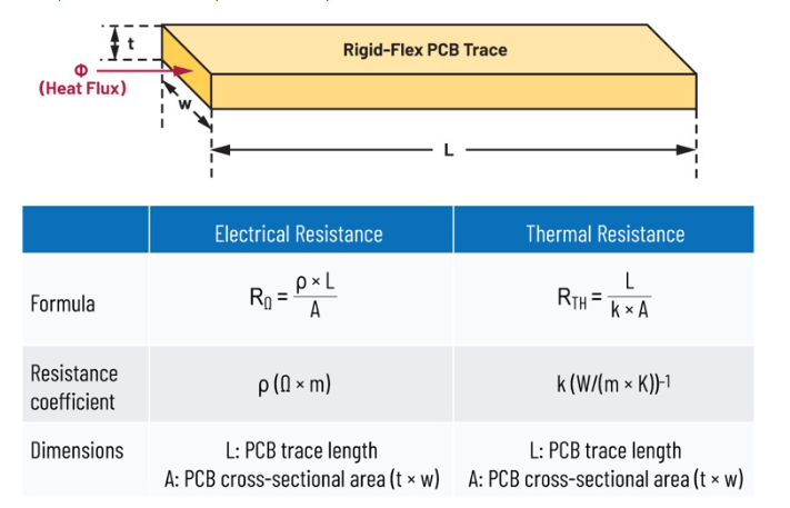
Figure 4. Electrical and thermal conductivity of PCB traces.
Before considering the thermal resistance of the PCB traces, we should first evaluate the thermal behavior of the conductive plug to establish a design baseline. The thermal conduction path of the conductive plug is cylindrical, as shown in Figure 5.
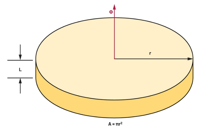
Figure 5. Thermal conduction of the conductive plug.
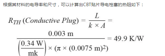
Based on the conductivity of its material and size, the thermal resistance of the CBT patch conductive plug can be calculated as follows:
When considering the thermal resistance of the PCB trace, we need to consider several issues:
The thermal resistance of the PCB trace should be significantly greater than the conductive plug of the CBT patch (for example, RTH(PCB trace) ≥ 100•RTH(conductive plug)).
The PCB trace size needs to be designed according to the power requirements of the temperature sensor (such as MAX30208) to minimize the heat loss from the trace to the CBT patch conductive plug. Using a low-power temperature sensor such as the MAX30208 can greatly reduce this heat loss.
It is also necessary to check whether there is potential heat radiation from the PCB trace in contact with the conductive core. The smaller the trace, the greater the I2R loss.
For a given cross-sectional area, the total length of the PCB trace should be sufficient to ensure a large thermal resistance compared to the CBT thermal plug.
Figure 6 shows the thermal/electrical properties of various commonly used PCB metals. Since the thermal and electrical conductivities of these metals (such as gold, copper, silver, and aluminum) are in the same order of magnitude, the specific material choice is not critical. Copper was chosen for its low cost, availability, and mechanical flexibility (discussed in the next section).
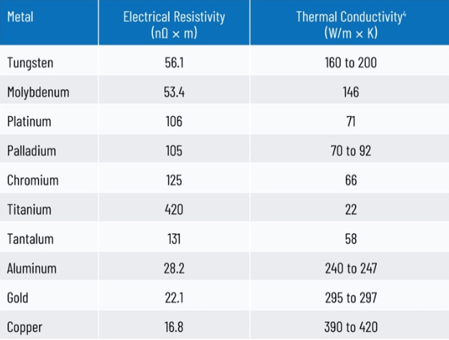
Figure 6. Electrical conductivity of common PCB metals.
Although the thermal conductivity of copper is more than 1000 times greater than that of the CBT patch plug, choosing smaller copper trace sizes can achieve thermal resistances much greater than 49.8 K/W (the thermal resistance of the CBT patch plug).
The PCB traces consist of a 1/2 ounce (17.3 micron thick) copper core, a 1.5 micron thick nickel layer, and a 0.1 micron thick gold plating layer. Given the relatively small size of the nickel and gold plating layers, which can be ignored, all subsequent calculations assume that the PCB traces consist of only the copper core.
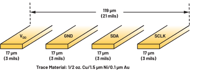
Figure 7. MAX30208 temperature sensor PCB power and signal traces.
Each PCB trace is 76.2 microns (3 mils) wide, which gives:
Note: Although we would like to use a smaller trace width to increase thermal resistance, the PCB manufacturer has restrictions on the minimum trace width. For example, we initially wanted a trace width of 2.5 mils, but ended up using the manufacturer’s recommended trace width of 3 mils.
In addition, since each MAX30208 temperature device requires four PCB traces of equal size (Figure 7), that is, four thermal paths in parallel, the overall PCB trace thermal resistance is also reduced by a factor of four, that is:

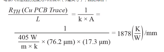
Figure 8 shows the approximate thermal resistance of the PCB traces from the four temperature sensors to the connector CN1.
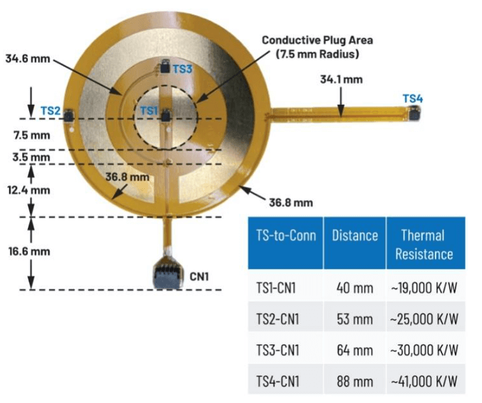
Figure 8. Estimated value of PCB trace thermal resistance.
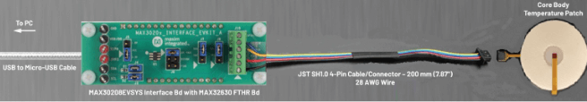
Figure 9. Connection of CBT patch to interface board.
As shown in Figure 8, the PCB trace with the lowest thermal resistance (such as TS1-CN1) is about 380 times greater than the thermal resistance of the CBT conductive plug, which meets the design goal of greater than or equal to 100 times. Additionally, an extension cable from connector CN1 to the MAX30208EVSYS interface board further improves performance. Our prototype system used a 200 mm (7.9 in) length of 28 AWG wire that was wrapped around the top of the ear pinna from the CBT patch to the interface board.
Note: While this thermal resistance is sufficient to isolate heat conduction within the conductive core, we still need to consider the heat generated by the interface board. If this heat is large enough, it can conduct back to the CBT patch and cause errors. The temperature sensor used in our evaluation system consumes very little power, so this is not an issue.
Reducing Thermal Errors in the Electrical System
When it comes to the electrical system, we will focus on two main areas: (1) heat generated by the MAX30208 device itself (i.e., self-heating), and (2) heat generated by the PCB traces (i.e., thermal radiation). Both of these heat sources can transfer heat to (or from) the CBT patch, which can adversely affect the thermal performance of the system. Figure 10 shows a simplified schematic of the MAX30208 circuit design.

The MAX30208 (±0.1°C accuracy, I2C) digital temperature sensor was chosen for its high accuracy and low power consumption. The CBT patch electrical system is powered by a 1.8 V regulated DC power supply on the MCU interface board. The I2C pull-up resistor is a significant source of heat and is located on the MCU board, not on the CBT patch rigid-flex PCB.
Table 1 lists the current and voltage specifications for each input/output pin when operating at 37°C. These values are derived from the electrical parameter table and related TOC data in the MAX30208 data sheet.

Figure 10. MAX30208 functional diagram.
Table 1. MAX30208 Input/Output Pin Voltage and Current Specifications
Rigid-Flex Circuit Design Considerations for Wearable Temperature Sensor Applications
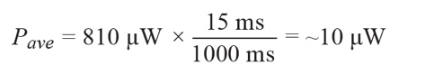
Therefore, most of the power consumption comes from the I2C signal lines and power supply, which consumes about 810 µW in continuous operation. Since the temperature signal does not change very quickly, periodic sampling can be used, which not only helps with data management, but also reduces overall power consumption, which in turn helps reduce heat dissipation in the MAX30208 device itself and the signal and power traces.
With an integration period of 15 ms and a sampling rate of 1 Hz, the average power dissipation of the MAX30208 is approximately:
Although the package thermal resistance is usually provided in the data sheet, designers must be cautious when using the package thermal resistance to estimate heat flow. This is because θjA (junction-to-ambient thermal resistance) and θjC (junction-to-case thermal resistance) are evaluated according to the JEDEC environment, which may be very different from the actual application. They are usually used to measure the quality factor of the chip when comparing between competing devices.
Therefore, we do not recommend using ambient temperature to infer the junction temperature,5 especially for the temperature sensor installed between insulating and non-insulating materials in this application.
Since the temperature measurement circuit of the MAX30208 relies on integrated circuit implementation, the first thing we need to pay attention to is the self-heating of the chip. The chip measures the external temperature on the top (or bottom) of the package, so assuming the case temperature is the same as the chip temperature, we can estimate the temperature error due to chip self-heating as follows6

This error is more than 100 times lower than the accuracy of the MAX30208 (for example, ±0.1°C), so we can accept the assumption made above that the case and chip temperatures are the same.
Note: This is not always possible when accurate chip temperature measurement is required. One technique that can be used is to use ESD diodes on the IC input/output lines as temperature sensors to measure the temperature rise of the IC chip.
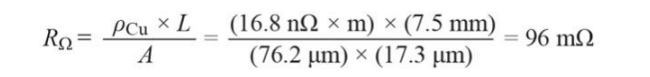
Next, we consider the I2R losses of the PCB traces in the conductive core area. As shown in Figure 8, the distance from TS1 or TS4 to the outer edge of the conductive core is 7.5 mm. Using the resistance formula for a single PCB trace (see Figure 4) and the conductivity of copper, we can calculate the following:
Since the maximum current of the SCL and SDA signal lines is 383 µApk, we calculate the error caused by thermal radiation from a single PCB trace as follows:
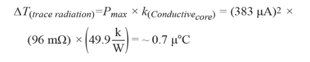
This is negligible for the thermal system in this example. For the case of periodic sampling, the error will be smaller than this. In summary, the thermal error due to the self-heating of the MAX30208 and the heat radiation of the conductive core PCB trace has little impact on the system.
At the same time, the line voltage drop is also within the acceptable range. The maximum length of the line is 88 mm (TS4 to CN1), plus 200 mm of 28 AWG wire (diameter 0.32 mm) connected to the MAX3020x interface board. Using the calculation formula for resistance, the following results can be calculated:

The maximum current of VDD is 67 µA, so the voltage drop of the line is as follows:

This voltage drop is small enough that there will be no power supply rejection issues.
The above are the main thermal and electrical design considerations for the rigid-flex PCB used in the CBT patch, but we still strongly recommend that a thermal finite element analysis (FEA) be performed to verify the transients before prototyping the first patch. Thermal capacitance and capacitance are not discussed in this article because they have little impact on performance in this application. However, we recommend that thermal capacitance and capacitance are also analyzed during the design stage.
Figure 11 shows the schematic diagram of the CBT device, highlighting how to achieve electrical interconnection and mitigate heat flow routing in a dual-layer polyimide rigid-flex PCB.
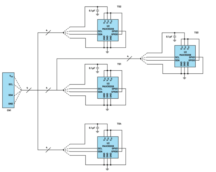
Figure 11. CBT patch schematic.
Layout design considerations to ensure mechanical reliability
The rigid-flex circuit uses a hybrid structure of traditional rigid PCB and flexible PCB. Although this circuit has mechanical flexibility to fit the human forehead, it needs to have mechanical rigidity in several key locations. They are:
- Nine SMT component connection points.
- Circuit contacts extending from the circular circuit area to the temperature sensor (TS4).
- Circuit contacts extending from the circular circuit area to the connector (CN1).
- Rigid-flex circuit boundary.
SMT components are usually connected using reflow soldering. Therefore, these components are usually mounted on rigid PCB material to maintain the integrity of the solder joints. Because flexible PCB materials require fewer stress reliefs, SMT components must be soldered carefully. Even if the system is relatively less physically disturbed, careful assembly is required to ensure long-term reliability.
Typical PCB reinforcements use FR4, polyamide, polyimide and/or metal. Our CBT patch uses 4 mils thick polyimide in the flexible area and 12 mils thick polyimide in the reinforced area. To increase rigidity, we reinforce the flexible contact circuit with metal sheets.
The CBT patch prototype will be made into a flat rigid-flex combination component and then subjected to two static bends. As shown in the figureAs shown in Figure 10, the circuit contacts extending from the circular circuit area to the TS4 temperature sensor require two 90-degree bends during final assembly.

Figure 12. Static bend of TS4 flexible circuit contacts.
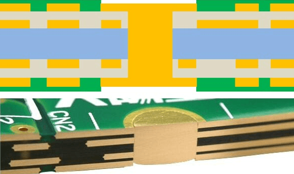
The TS4 flexible circuit contact design uses a brick-patterned metal sheet to reduce metal fatigue caused by a single static bend. Figure 13 shows these staggered brick-pattern reinforcements that can reduce mechanical stress at the rigid-flex boundary. In addition, the intermittent brick pattern can also eliminate thermal conduction along these metal paths. This design technique is also used for the circuit contacts extending from the circular circuit area to the connector (CN1)

.
Figure 13. Staggered brick-patterned flexible contact reinforcements.
Other aspects to consider include avoiding 90-degree corners (such as stress concentration points) and the installation of prefabricated parts.
Manufacturing Considerations and Guidelines
To design a stable and reliable product, we recommend that designers work closely with the PCB assembly house. All electrical, thermal, and mechanical design details should be reviewed before the first device is manufactured. In many cases, manufacturers have alternative materials and/or techniques that can be used to improve the design.
During the development of the rigid-flex PCB assembly process for the CBT patch, several significant challenges caused by the use of reflow materials and reflow profiles had to be overcome. We initially used standard reflow solder, which resulted in delamination of the PCB (see Figure 14). As an insulator, air pockets affect the heat flow through the rigid-flex PCB, which is particularly detrimental to thermal design. We ultimately mitigated this issue by using an alternative low-temperature eutectic solder. The reflow profile had to be fine-tuned several times to achieve acceptable yield.
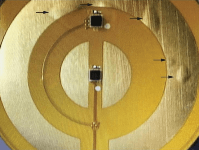
Figure 14. Rigid-flex PCB delamination for CBT patch.
Conclusion
This article discusses design considerations to help address the technical challenges of high-precision heat flow applications, namely how to use high-precision, low-power devices (such as the MAX30208 temperature sensor) to meet the performance requirements of the core body temperature patch. A successful design can be achieved by selecting the right components and applying good design techniques to properly balance the performance between thermal, electrical, and mechanical.