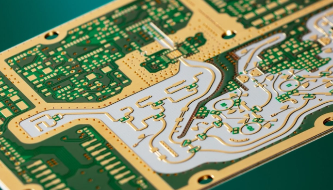
Switch Mode Power Supply PCB Layout Techniques
Abstract
Switch Mode Power Supplies (SMPS) are widely used in modern electronics due to their high efficiency, compact size, and ability to handle varying input voltages. However, achieving optimal performance requires careful PCB (Printed Circuit Board) layout design. Poor PCB layout can lead to issues such as electromagnetic interference (EMI), excessive noise, thermal problems, and even circuit failure. This paper discusses key PCB layout techniques for SMPS, including component placement, grounding strategies, trace routing, thermal management, and EMI reduction.
1. Introduction
Switch Mode Power Supplies convert electrical power efficiently by rapidly switching transistors between on and off states. The high-frequency switching introduces challenges in PCB design, including noise coupling, voltage spikes, and thermal dissipation. A well-designed PCB layout ensures stable operation, minimizes losses, and complies with electromagnetic compatibility (EMC) standards.
2. Key Considerations in SMPS PCB Layout
2.1 Component Placement
Proper component placement is crucial for minimizing parasitic inductance and resistance. Key guidelines include:
- Power Stage Components (MOSFETs, Diodes, Inductors, Transformers):
- Place switching components close to each other to minimize loop area.
- Position high-current paths with short and wide traces.
- Control Circuit (PWM Controller, Feedback Network):
- Keep sensitive analog components away from noisy switching sections.
- Use ground planes to shield control signals.
- Input/Output Capacitors:
- Place input capacitors near the switching FETs to reduce high-frequency noise.
- Position output capacitors close to the load to improve transient response.
2.2 Grounding Strategies
Grounding in SMPS must handle both high-frequency switching noise and low-frequency return currents.
- Star Grounding:
- Connect all ground returns to a single point to avoid ground loops.
- Split Ground Planes:
- Use separate analog and power ground planes, connected at a single point.
- Minimizing Ground Impedance:
- Use wide traces or ground pours for high-current return paths.
2.3 Trace Routing
- High-Current Traces:
- Use thick traces (≥ 20 mils) to reduce resistance and inductance.
- Avoid sharp bends; use 45° angles or curves.
- High-Frequency Switching Nodes:
- Keep traces short to minimize parasitic inductance.
- Avoid running switching traces parallel to sensitive signal lines.
- Signal Traces (Feedback, PWM):
- Route them away from noisy areas.
- Use guard traces or ground shielding if necessary.
2.4 Thermal Management
SMPS components generate significant heat, requiring proper thermal design:
- Copper Pour for Heat Dissipation:
- Use large copper areas for power components (MOSFETs, diodes).
- Thermal Vias:
- Place multiple vias under hot components to transfer heat to inner layers.
- Heatsinks:
- Attach heatsinks to high-power devices if needed.
2.5 EMI Reduction Techniques
High-frequency switching generates EMI, which must be minimized for compliance with regulatory standards (e.g., FCC, CISPR).
- Loop Area Minimization:
- Small loops reduce radiated emissions.
- Shielding:
- Use grounded metal shields for sensitive circuits.
- Filtering:
- Add ferrite beads and EMI filters at input/output stages.
- Proper Decoupling:
- Place decoupling capacitors close to IC power pins.
3. Practical PCB Layout Example
Consider a buck converter layout:
- Input Stage:
- Place input capacitors near the MOSFETs.
- Use thick traces for Vin and ground.
- Switching Node:
- Keep the connection between MOSFET, diode, and inductor short.
- Output Stage:
- Position output capacitors near the load.
- Control Circuit:
- Route feedback traces away from switching noise.
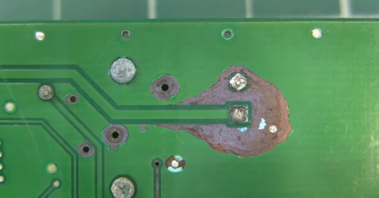
4. Common Mistakes in SMPS PCB Layout
- Long High-Current Traces: Increases resistance and EMI.
- Improper Grounding: Causes noise coupling and instability.
- Insufficient Decoupling: Leads to voltage spikes and oscillations.
- Poor Thermal Design: Results in overheating and reduced reliability.
5. Conclusion
An optimized PCB layout is essential for the reliable operation of Switch Mode Power Supplies. By following best practices in component placement, grounding, trace routing, thermal management, and EMI reduction, designers can achieve high efficiency, low noise, and compliance with industry standards. Careful simulation and prototyping further validate the design before mass production.


