Thermal Design Planning in PCB Design: Strategies and Best Practices
Introduction
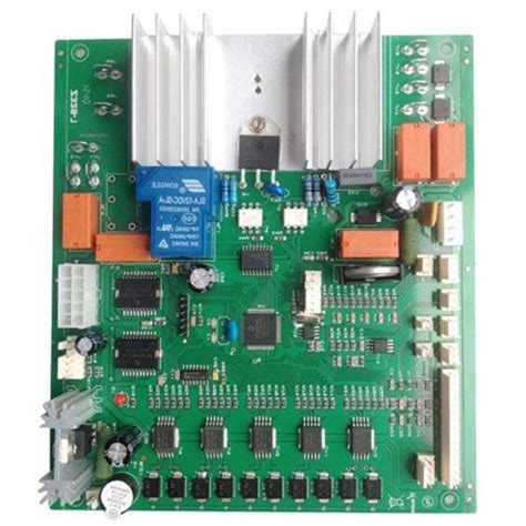
Printed Circuit Board (PCB) design has evolved significantly with the increasing complexity and miniaturization of electronic devices. One critical aspect that often determines the reliability and performance of electronic systems is thermal management. Effective thermal design planning in PCB design ensures that components operate within their specified temperature ranges, preventing premature failure and maintaining optimal performance. This 2000-word article explores the fundamental principles, strategies, and best practices for thermal design in PCB development.
The Importance of Thermal Design in PCBs
Thermal management in PCB design addresses the heat generated by electronic components during operation. As electronic devices become more powerful and compact, the power density increases, making thermal considerations more crucial than ever. Poor thermal design can lead to:
- Component degradation and reduced lifespan
- Thermal stress leading to mechanical failures
- Performance throttling in processors and other ICs
- Potential safety hazards from excessive heat
- Increased failure rates and reduced product reliability
Proper thermal planning must begin early in the design process and continue throughout the PCB development lifecycle to ensure optimal thermal performance.
Fundamental Principles of PCB Thermal Management
Heat Transfer Mechanisms
Understanding the three primary heat transfer mechanisms is essential for effective thermal design:
- Conduction: Heat transfer through solid materials (PCB substrate, copper traces, thermal vias)
- Convection: Heat transfer to surrounding air or liquid (natural or forced convection)
- Radiation: Electromagnetic wave heat transfer (typically less significant in PCBs)
Thermal Resistance Network
Every PCB can be modeled as a thermal resistance network where:
- θJA (Junction-to-Ambient) represents total thermal resistance
- θJC (Junction-to-Case) represents resistance from die to package surface
- θCA (Case-to-Ambient) represents resistance from package to environment
Designers must minimize these resistances through careful material selection and layout strategies.
Thermal Design Planning Process
1. Early-Stage Thermal Analysis
Begin thermal planning during the schematic design phase by:
- Identifying high-power components and their thermal characteristics
- Estimating power dissipation for all critical components
- Considering the operating environment (ambient temperature, airflow conditions)
- Reviewing manufacturer thermal specifications for all components
2. Component Placement Strategies
Optimal component placement significantly impacts thermal performance:
- Distribute heat-generating components across the board
- Avoid clustering high-power devices
- Place temperature-sensitive components away from heat sources
- Consider the natural airflow path in the enclosure
- Orient components to maximize heat dissipation

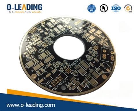
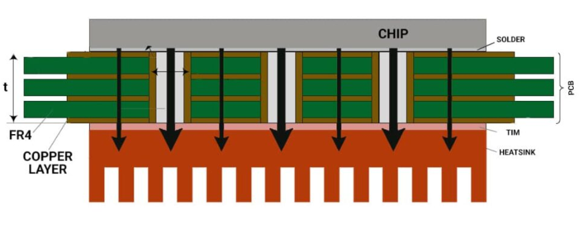
3. PCB Stackup Design for Thermal Management
The PCB stackup affects thermal performance:
- Use thicker copper layers for high-current traces (2oz or more)
- Incorporate dedicated power and ground planes for heat spreading
- Consider using thermal vias under high-power components
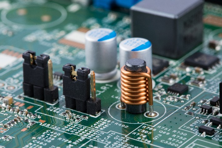
- Select appropriate substrate materials (high thermal conductivity when needed)
4. Copper Pour and Thermal Relief
Proper use of copper features enhances heat dissipation:
- Implement large copper pours connected to component thermal pads
- Use thermal relief connections to balance soldering and heat transfer
- Create copper heat spreaders for localized hot spots
- Connect copper pours to internal planes when possible
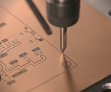
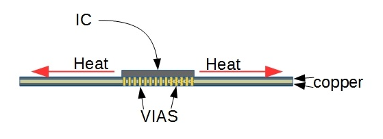
5. Via Strategies for Heat Transfer
Thermal vias are crucial for transferring heat between layers:
- Place arrays of thermal vias under high-power components
- Optimize via diameter and plating thickness
- Consider filled vias for improved thermal performance
- Connect vias to internal ground or power planes
6. Solder Mask Considerations
Solder mask affects heat dissipation:
- Expose copper areas for better heat radiation
- Use selective solder mask opening for thermal pads
- Consider thermal conductivity of solder mask material
Advanced Thermal Management Techniques
1. Embedded Heat Spreaders
For extremely high-power applications:
- Incorporate metal cores or inserts
- Use embedded heat pipes or vapor chambers
- Implement direct bonded copper (DBC) substrates
2. Thermal Interface Materials (TIMs)
Select appropriate TIMs for component-to-heatsink interfaces:
- Thermal pads, greases, or phase-change materials
- Consider long-term stability and pump-out effects
- Optimize thickness for minimum thermal resistance
3. Active Cooling Integration
When passive cooling is insufficient:
- Design for fan mounting and airflow
- Incorporate Peltier coolers for precise temperature control
- Consider liquid cooling solutions for extreme applications
Thermal Simulation and Analysis
Modern PCB design benefits from thermal simulation tools:
- Finite Element Analysis (FEA) for detailed thermal modeling
- Computational Fluid Dynamics (CFD) for airflow analysis
- Transient thermal analysis for dynamic conditions
- Coupled electrical-thermal simulations
Perform thermal simulations at multiple design stages to validate thermal performance and identify potential issues early.
Design for Manufacturing (DFM) Thermal Considerations
Ensure thermal design aligns with manufacturing capabilities:
- Verify copper balance to prevent warpage
- Consider thermal expansion mismatches
- Account for soldering process temperatures
- Evaluate rework implications of thermal features
Testing and Validation
After manufacturing, validate thermal performance:
- Infrared thermography for temperature mapping
- Thermocouple measurements at critical points
- Environmental stress testing
- Long-term reliability testing
Industry Standards and Guidelines
Follow relevant standards for thermal design:
- IPC-2152 for current carrying capacity and thermal relationships
- JEDEC standards for component thermal characterization
- Military and automotive specifications for harsh environments
Future Trends in PCB Thermal Design
Emerging technologies are shaping thermal management:
- Advanced thermally conductive substrate materials
- 3D-printed heat dissipation structures
- Nanomaterials for enhanced thermal interfaces
- AI-driven thermal optimization algorithms
Conclusion
Effective thermal design planning is a critical aspect of modern PCB development that directly impacts product reliability, performance, and longevity. By incorporating thermal considerations from the earliest design stages, employing appropriate heat dissipation techniques, and validating through simulation and testing, designers can create PCBs that meet both electrical and thermal requirements. As electronic devices continue to push performance boundaries while shrinking in size, innovative thermal management solutions will remain essential for successful PCB design.
The strategies outlined in this article provide a comprehensive framework for addressing thermal challenges in PCB design. By implementing these best practices and staying informed about emerging technologies, design engineers can develop robust solutions that effectively manage heat in even the most demanding applications.