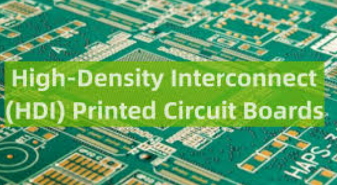
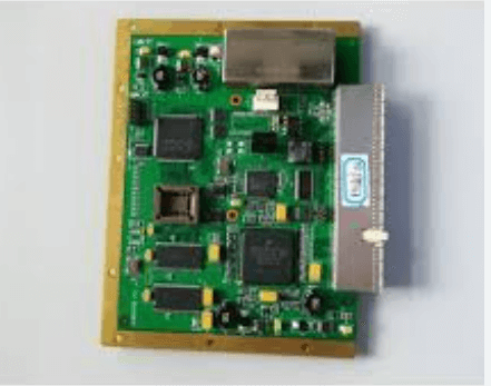
Types of hdi pcb
Advantages Of Single-Sided HDI PCBs
Single-sided High-Density Interconnect (HDI) Printed Circuit Boards (PCBs) have become increasingly popular in the electronics industry due to their numerous advantages. These PCBs are characterized by their high wiring density per unit area, which is achieved through the use of microvias, fine lines, and high-performance thin materials. As a result, single-sided HDI PCBs offer several benefits that make them an attractive choice for various applications.
One of the primary advantages of single-sided HDI PCBs is their ability to support miniaturization.
In today’s world, where electronic devices are becoming smaller and more compact, the need for miniaturized components is paramount. Single-sided HDI PCBs allow for the integration of more components in a smaller area, thereby enabling the design of compact and lightweight devices. This is particularly beneficial for industries such as consumer electronics, medical devices, and aerospace, where space and weight constraints are critical considerations.
In addition to supporting miniaturization, single-sided HDI PCBs also offer improved electrical performance.
The use of microvias and fine lines reduces the length of electrical paths, which in turn minimizes signal loss and enhances signal integrity. This is especially important in high-frequency applications, where maintaining signal integrity is crucial for optimal performance. Furthermore, the reduced electrical path length also contributes to lower power consumption, making single-sided HDI PCBs an energy-efficient option.
Another significant advantage of single-sided HDI PCBs is their cost-effectiveness.
While the initial manufacturing cost of HDI PCBs may be higher compared to traditional PCBs, the overall cost savings can be substantial. The ability to integrate more components on a single layer reduces the need for additional layers, which can significantly lower the material and production costs. Moreover, the enhanced reliability and performance of single-sided HDI PCBs can lead to reduced maintenance and repair costs over the product’s lifecycle.
The reliability of single-sided HDI PCBs is another noteworthy benefit.
The use of advanced materials and manufacturing techniques ensures that these PCBs can withstand harsh environmental conditions and mechanical stresses. This makes them suitable for applications in demanding environments, such as automotive and industrial sectors. Additionally, the high-quality construction of single-sided HDI PCBs minimizes the risk of defects and failures, thereby enhancing the overall reliability and longevity of the electronic devices in which they are used.
Furthermore, single-sided HDI PCBs offer greater design flexibility.
The ability to incorporate microvias and fine lines allows designers to create complex and intricate circuit patterns that would be challenging to achieve with traditional PCBs. This flexibility enables the development of innovative and high-performance electronic products that meet the evolving needs of various industries. Additionally, the use of advanced design software and simulation tools further enhances the design process, allowing for the optimization of PCB layouts and ensuring that the final product meets the desired specifications.
In conclusion, single-sided HDI PCBs provide a multitude of advantages that make them a preferred choice for modern electronic applications. Their support for miniaturization, improved electrical performance, cost-effectiveness, reliability, and design flexibility make them an invaluable asset in the development of cutting-edge electronic devices. As technology continues to advance, the demand for single-sided HDI PCBs is expected to grow, further solidifying their importance in the electronics industry.
Benefits Of Double-Sided HDI PCBs
Double-sided High-Density Interconnect (HDI) Printed Circuit Boards (PCBs) have become increasingly popular in the electronics industry due to their numerous advantages. These advanced PCBs are designed to accommodate more components in a smaller area, making them ideal for modern electronic devices that demand compactness and high performance.
One of the primary benefits of double-sided HDI PCBs is their ability to support higher component density.
By utilizing both sides of the board, designers can place more components in a limited space, which is crucial for miniaturized devices such as smartphones, tablets, and wearable technology. This increased component density not only saves space but also enhances the overall functionality of the device.
In addition to supporting higher component density, double-sided HDI PCBs offer improved electrical performance.
The use of microvias, which are smaller than traditional vias, allows for shorter and more direct routing of electrical signals. This results in reduced signal loss and lower electromagnetic interference (EMI), leading to better signal integrity and faster data transmission. Consequently, devices that incorporate double-sided HDI PCBs can achieve higher performance levels and greater reliability. Another significant advantage of double-sided HDI PCBs is their enhanced thermal management capabilities. The increased number of layers and the use of advanced materials help to dissipate heat more effectively, preventing overheating and ensuring the longevity of the components. This is particularly important for high-power applications where efficient heat dissipation is critical to maintaining optimal performance and preventing damage to sensitive components.
Moreover, double-sided HDI PCBs contribute to cost savings in the long run.
Although the initial manufacturing cost may be higher due to the complexity of the design and the use of advanced materials, the overall cost of production can be reduced. This is because the compact design of double-sided HDI PCBs allows for smaller and lighter devices, which in turn reduces shipping and handling costs. Additionally, the improved reliability and performance of these PCBs can lead to fewer failures and lower maintenance costs over the device’s lifespan.
The versatility of double-sided HDI PCBs is another noteworthy benefit.
They can be used in a wide range of applications, from consumer electronics to industrial and medical devices. Their ability to support complex circuitry and high-speed data transmission makes them suitable for advanced applications such as 5G technology, Internet of Things (IoT) devices, and automotive electronics. This versatility ensures that double-sided HDI PCBs will continue to play a crucial role in the development of cutting-edge technologies.
Furthermore, the use of double-sided HDI PCBs aligns with the growing trend towards environmentally friendly and sustainable manufacturing practices. The compact design and efficient use of materials result in less waste and a smaller environmental footprint. Additionally, the improved thermal management and reliability of these PCBs contribute to longer device lifespans, reducing the need for frequent replacements and minimizing electronic waste. In conclusion, double-sided HDI PCBs offer a multitude of benefits that make them an attractive choice for modern electronic devices. Their ability to support higher component density, improved electrical performance, enhanced thermal management, cost savings, versatility, and environmental sustainability make them a valuable asset in the electronics industry. As technology continues to advance, the demand for double-sided HDI PCBs is expected to grow, further solidifying their importance in the development of innovative and high-performance electronic devices.
Applications Of Multilayer HDI PCBs
High-Density Interconnect (HDI) printed circuit boards (PCBs) have become a cornerstone in modern electronics, offering numerous advantages over traditional PCBs. Among the various types of HDI PCBs, multilayer HDI PCBs stand out due to their ability to support complex circuitry in a compact form. The applications of multilayer HDI PCBs are vast and varied, spanning multiple industries and technological domains. Understanding these applications provides insight into why these advanced PCBs are indispensable in today’s high-tech world.
One of the primary applications of multilayer HDI PCBs is in the consumer electronics industry.
Devices such as smartphones, tablets, and laptops require compact, efficient, and reliable circuitry to function effectively. Multilayer HDI PCBs meet these requirements by allowing for more components to be placed in a smaller area, thereby reducing the overall size and weight of the device. This miniaturization is crucial for portable electronics, where space is at a premium and performance cannot be compromised. Additionally, the enhanced electrical performance of multilayer HDI PCBs ensures that these devices can handle high-speed data transmission and complex processing tasks without significant signal loss or interference.
Transitioning to the automotive industry, multilayer HDI PCBs play a critical role in the development of advanced driver-assistance systems (ADAS) and infotainment systems.
Modern vehicles are equipped with numerous electronic components that enhance safety, navigation, and entertainment. Multilayer HDI PCBs enable the integration of these components into a cohesive system, ensuring reliable performance under various operating conditions. The ability to withstand high temperatures and vibrations makes these PCBs ideal for automotive applications, where durability and reliability are paramount.
In the realm of medical devices, the precision and reliability of multilayer HDI PCBs are indispensable.
Medical equipment such as diagnostic imaging systems, patient monitoring devices, and portable medical instruments rely on these advanced PCBs to function accurately and efficiently. The compact size of multilayer HDI PCBs allows for the development of smaller, more portable medical devices, which can be crucial in emergency situations or for home healthcare applications. Furthermore, the high reliability of these PCBs ensures that medical devices can operate without failure, which is critical in life-saving scenarios.
The aerospace and defense sectors also benefit significantly from the use of multilayer HDI PCBs.
In these industries, the need for high-performance, reliable, and compact electronic systems is paramount. Multilayer HDI PCBs are used in a variety of applications, including communication systems, navigation systems, and control systems for aircraft and defense equipment. The ability to handle high-frequency signals and the robustness of these PCBs make them suitable for the demanding environments encountered in aerospace and defense applications.
Moreover, the telecommunications industry leverages the advantages of multilayer HDI PCBs to support the infrastructure required for high-speed data transmission and communication networks. Base stations, routers, and switches all utilize these advanced PCBs to ensure efficient and reliable data processing and transmission. The high-density interconnects facilitate the handling of large volumes of data at high speeds, which is essential for maintaining the performance and reliability of modern communication networks.
In conclusion, the applications of multilayer HDI PCBs are extensive and critical across various industries. From consumer electronics to automotive, medical, aerospace, defense, and telecommunications, these advanced PCBs provide the necessary performance, reliability, and compactness required in today’s technologically driven world. The continuous advancements in HDI PCB technology promise to further expand their applications, driving innovation and efficiency across multiple domains.
Innovations In Rigid-Flex HDI PCBs
High-Density Interconnect (HDI) printed circuit boards (PCBs) have revolutionized the electronics industry by enabling the development of more compact, efficient, and high-performance devices.
Among the various types of HDI PCBs, rigid-flex HDI PCBs stand out due to their unique combination of flexibility and rigidity, which offers unparalleled design versatility and reliability. These innovations in rigid-flex HDI PCBs have opened new avenues for applications in various sectors, including consumer electronics, medical devices, aerospace, and automotive industries.
Rigid-flex HDI PCBs are composed of both rigid and flexible substrates, seamlessly integrated into a single unit.
This hybrid structure allows for the creation of complex circuits that can be folded or bent without compromising the integrity of the connections. The rigid sections provide structural support and house components that require a stable platform, while the flexible sections enable dynamic movement and connectivity in confined spaces. This combination is particularly advantageous in applications where space constraints and mechanical stress are significant considerations.
One of the primary innovations in rigid-flex HDI PCBs is the use of microvias, which are tiny holes that connect different layers of the PCB.
Microvias are essential in HDI technology as they allow for higher wiring density and more efficient use of the available space. By employing laser drilling techniques, manufacturers can create microvias with diameters as small as 50 micrometers, significantly enhancing the interconnectivity and performance of the PCB. This advancement has been crucial in meeting the demands of modern electronic devices, which require increasingly smaller and more powerful components.
Another significant development in rigid-flex HDI PCBs is the implementation of advanced materials and fabrication processes.
The use of high-performance polymers and adhesives ensures that the flexible sections maintain their integrity and functionality under various environmental conditions. Additionally, advancements in lamination techniques have improved the bonding between the rigid and flexible layers, resulting in more robust and reliable PCBs. These material and process innovations have extended the lifespan and durability of rigid-flex HDI PCBs, making them suitable for critical applications where reliability is paramount.
The integration of embedded components is another noteworthy innovation in rigid-flex HDI PCBs.
By embedding passive and active components within the layers of the PCB, designers can further reduce the overall size and weight of the device. This approach not only saves space but also enhances the electrical performance by minimizing signal loss and improving thermal management. Embedded components are particularly beneficial in applications such as wearable devices and medical implants, where miniaturization and performance are critical.
Moreover, the advancements in computer-aided design (CAD) tools have significantly contributed to the evolution of rigid-flex HDI PCBs.
Modern CAD software allows for precise modeling and simulation of complex PCB designs, enabling engineers to optimize the layout and performance before fabrication. This capability reduces the risk of errors and accelerates the development process, ensuring that the final product meets the stringent requirements of today’s electronic devices.
In conclusion, the innovations in rigid-flex HDI PCBs have transformed the landscape of electronic design and manufacturing. The combination of rigid and flexible substrates, coupled with advancements in microvia technology, materials, fabrication processes, embedded components, and CAD tools, has resulted in highly versatile and reliable PCBs. These developments have not only enhanced the performance and miniaturization of electronic devices but also expanded the possibilities for new applications across various industries. As technology continues to evolve, rigid-flex HDI PCBs will undoubtedly play a pivotal role in shaping the future of electronics.