What is pcb assembly
Introduction To PCB Assembly: Understanding The Basics
Printed Circuit Board (PCB) assembly is a critical process in the manufacturing of electronic devices, serving as the backbone for most electronic circuits. Understanding the basics of PCB assembly is essential for anyone involved in electronics design, manufacturing, or repair. This process involves several steps, each crucial to ensuring the functionality and reliability of the final product.
To begin with, PCB assembly starts with the design and fabrication of the PCB itself.
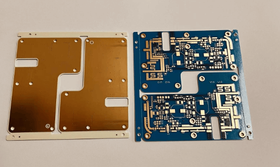
The PCB is a flat board made of non-conductive material, typically fiberglass, with conductive pathways etched or printed onto its surface. These pathways, or traces, connect various electronic components, allowing them to communicate and function together. The design phase involves creating a schematic diagram and layout, which are then used to produce the physical board through a process called PCB fabrication.
Once the PCB is fabricated, the next step is to assemble the electronic components onto the board.
This is where PCB assembly truly begins. Components such as resistors, capacitors, integrated circuits, and connectors are placed on the board in their designated positions. There are two primary methods for placing components: through-hole technology (THT) and surface-mount technology (SMT). THT involves inserting component leads through holes in the PCB and soldering them on the opposite side, while SMT involves placing components directly onto the surface of the PCB and soldering them in place.
The choice between THT and SMT depends on various factors, including the type of components used, the complexity of the circuit, and the intended application of the final product. SMT is generally preferred for modern electronics due to its ability to accommodate smaller components and higher circuit densities. However, THT is still used for components that require a stronger mechanical bond or for applications where high power or high voltage is involved.
After the components are placed, the next step is soldering, which secures the components to the PCB and establishes electrical connections.
Soldering can be done manually or through automated processes such as wave soldering or reflow soldering. In wave soldering, the PCB is passed over a wave of molten solder, which adheres to the exposed metal surfaces. Reflow soldering, on the other hand, involves applying solder paste to the PCB, placing the components, and then heating the assembly in a reflow oven to melt the solder and create the connections.
Following soldering, the assembled PCB undergoes inspection and testing to ensure that all components are correctly placed and properly soldered.
Automated optical inspection (AOI) and X-ray inspection are commonly used to detect defects such as misaligned components, solder bridges, and insufficient solder joints. Functional testing is also performed to verify that the assembled PCB operates as intended.
In conclusion, PCB assembly is a multifaceted process that involves designing the PCB, placing components, soldering, and rigorous inspection and testing. Each step is vital to the production of reliable and functional electronic devices. As technology continues to advance, the methods and techniques used in PCB assembly are continually evolving, making it an ever-important field in the electronics industry. Understanding the basics of PCB assembly provides a foundation for further exploration and innovation in this essential area of technology.
The Step-By-Step Process Of PCB Assembly
Printed Circuit Board (PCB) assembly is a meticulous process that involves several stages, each crucial to the creation of a functional electronic device. The process begins with the design and fabrication of the PCB itself. Engineers use specialized software to design the circuit layout, ensuring that all components will fit and function correctly. Once the design is finalized, the PCB is fabricated, typically using a combination of etching and layering techniques to create the necessary conductive pathways.
Following the fabrication of the PCB, the next step is the application of solder paste.
Solder paste, a mixture of tiny solder balls and flux, is applied to the board using a stencil that matches the design layout. This paste is essential for securing the electronic components to the board. The application must be precise, as any misalignment can lead to defects in the final product.
Once the solder paste is in place, the process moves on to component placement
This step involves placing various electronic components, such as resistors, capacitors, and integrated circuits, onto the board. Modern PCB assembly often utilizes automated machines known as pick-and-place machines for this task. These machines are programmed to place components with high accuracy and speed, significantly reducing the likelihood of human error.
After the components are placed, the assembly undergoes a reflow soldering process.
During reflow soldering, the board is passed through a specialized oven where it is gradually heated to melt the solder paste. This process ensures that the components are securely attached to the board. The temperature profile of the oven is carefully controlled to prevent damage to the components and the board itself.
Following reflow soldering, the assembly is inspected for any defects.
This inspection can be performed using various methods, including visual inspection, automated optical inspection (AOI), and X-ray inspection. Visual inspection is often used for simpler boards, while AOI and X-ray inspection are employed for more complex assemblies. These methods help identify issues such as solder bridges, missing components, and misalignments.
If any defects are found during inspection, the board may undergo rework or repair.
Rework involves removing and replacing defective components, while repair may involve correcting soldering issues. This step is crucial for ensuring the reliability and functionality of the final product.
Once the board passes inspection, it moves on to the final assembly stage, where additional components such as connectors and heat sinks may be added. This stage also includes functional testing, where the board is powered on and tested to ensure it operates as intended. Functional testing can involve a variety of tests, including electrical tests, software tests, and environmental tests, depending on the specific requirements of the product.
The final step in the PCB assembly process is packaging and shipping.
The assembled boards are carefully packaged to protect them from damage during transit. Proper packaging is essential to maintain the integrity of the boards and ensure they arrive at their destination in optimal condition.
In conclusion, PCB assembly is a complex and multi-faceted process that requires precision and attention to detail at every stage. From design and fabrication to component placement, soldering, inspection, and final assembly, each step is critical to producing a reliable and functional electronic device. The use of advanced technologies and automated systems has significantly improved the efficiency and accuracy of PCB assembly, making it possible to produce high-quality electronic products on a large scale.
Key Components Involved In PCB Assembly
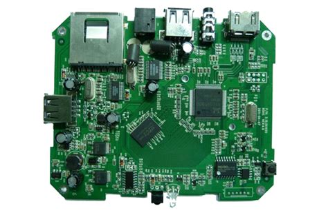
Printed Circuit Board (PCB) assembly is a critical process in the manufacturing of electronic devices, involving the integration of various components onto a PCB to create a functional electronic circuit. Understanding the key components involved in PCB assembly is essential for grasping the intricacies of this process. The primary components include the PCB itself, electronic components, solder paste, and various assembly equipment.
The PCB serves as the foundation for the entire assembly process.
It is a flat, insulating board made from materials such as fiberglass or composite epoxy, with conductive pathways etched or printed onto its surface. These pathways, or traces, connect different electronic components, allowing electrical signals to flow between them. The design and layout of the PCB are crucial, as they determine the efficiency and functionality of the final product.
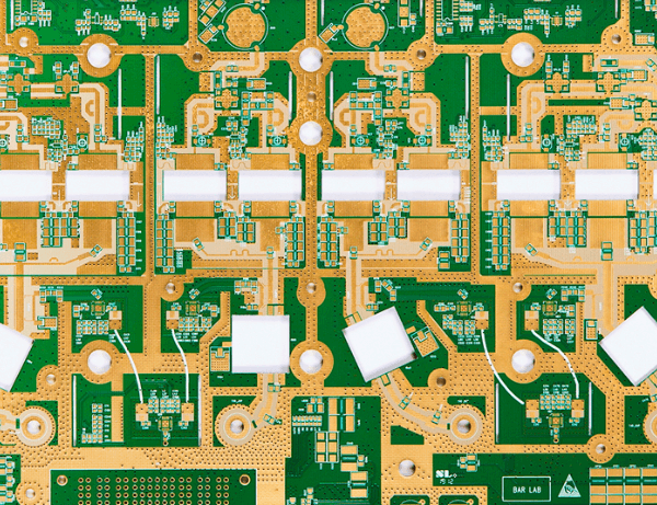
Electronic components are the building blocks of any PCB assembly.
These components can be broadly categorized into passive and active components. Passive components, such as resistors, capacitors, and inductors, do not require an external power source to operate. They perform essential functions like filtering, storing energy, and controlling current flow. Active components, on the other hand, include transistors, diodes, and integrated circuits (ICs). These components require an external power source and are responsible for amplifying signals, switching, and processing data. The selection and placement of these components are vital for the performance and reliability of the assembled PCB.
Solder paste is another crucial element in PCB assembly.
It is a mixture of tiny solder balls and flux, which is applied to the PCB’s surface using a stencil. The solder paste serves as an adhesive, holding the electronic components in place before they are permanently attached through a process called reflow soldering. During reflow soldering, the PCB is heated in a controlled environment, causing the solder paste to melt and form a strong, conductive bond between the components and the PCB. The quality of the solder paste and the precision of its application are critical factors in ensuring a reliable connection.
Assembly equipment plays a significant role in the PCB assembly process.
Surface Mount Technology (SMT) machines are commonly used to place electronic components onto the PCB with high accuracy and speed. These machines pick components from reels or trays and place them onto the PCB according to the design specifications. Additionally, through-hole technology (THT) equipment is used for components with leads that need to be inserted into holes on the PCB. These components are then soldered in place using wave soldering or selective soldering techniques.
Inspection and testing are also integral components of the PCB assembly process.
Automated Optical Inspection (AOI) systems are employed to check for defects such as misaligned components, soldering issues, and other anomalies. X-ray inspection systems can be used to examine hidden solder joints and internal structures of the PCB. Functional testing ensures that the assembled PCB operates as intended, verifying the performance of the electronic components and the overall circuit.
In conclusion, PCB assembly is a complex process that involves several key components working in harmony. The PCB itself, electronic components, solder paste, and assembly equipment all play vital roles in creating a functional and reliable electronic circuit. Understanding these components and their interactions is essential for anyone involved in the design, manufacturing, or quality assurance of electronic devices.
Common Challenges And Solutions In PCB Assembly
Printed Circuit Board (PCB) assembly is a critical process in the manufacturing of electronic devices, involving the mounting of electronic components onto a PCB to create a functional circuit. Despite its importance, PCB assembly is fraught with numerous challenges that can impact the quality, reliability, and performance of the final product. Understanding these common challenges and their solutions is essential for ensuring successful PCB assembly.
One of the primary challenges in PCB assembly is component placement accuracy.
As electronic devices become more compact and complex, the need for precise placement of components on the PCB becomes increasingly critical. Misalignment or incorrect placement can lead to short circuits, signal integrity issues, and overall device malfunction. To address this challenge, advanced pick-and-place machines equipped with high-resolution cameras and sophisticated algorithms are employed. These machines ensure that components are placed with high precision, reducing the likelihood of errors.
Another significant challenge is soldering defects, which can manifest as solder bridges, cold joints, or insufficient solder.
These defects can compromise the electrical connections between components and the PCB, leading to intermittent or complete failure of the device. To mitigate soldering defects, manufacturers utilize automated soldering techniques such as reflow soldering and wave soldering. Additionally, implementing stringent process controls and regular inspection using X-ray or automated optical inspection (AOI) systems can help identify and rectify soldering issues early in the assembly process.
Thermal management is also a critical concern in PCB assembly, particularly for high-power applications.
Inadequate thermal management can result in overheating, which can damage components and reduce the lifespan of the device. To address this, designers incorporate thermal vias, heat sinks, and thermal pads into the PCB layout to facilitate efficient heat dissipation. Moreover, selecting components with appropriate thermal ratings and using thermal interface materials can further enhance thermal management.
Electrostatic discharge (ESD) is another challenge that can adversely affect PCB assembly.
ESD can damage sensitive electronic components, leading to latent defects that may not be immediately apparent but can cause device failure over time. To prevent ESD-related issues, manufacturers implement ESD control measures such as grounding wrist straps, ESD-safe workstations, and ionizers. Additionally, using ESD-safe packaging materials during component storage and transportation can help protect components from electrostatic damage.
Component availability and supply chain management also pose significant challenges in PCB assembly.
The global electronics industry is highly dynamic, with frequent changes in component availability and lead times. Shortages or delays in component supply can disrupt the assembly process and extend production timelines. To mitigate these risks, manufacturers adopt strategies such as maintaining buffer stocks, establishing relationships with multiple suppliers, and using alternative components that meet the same specifications.
Finally, ensuring compliance with industry standards and regulations is crucial in PCB assembly.
Standards such as IPC-A-610 and ISO 9001 provide guidelines for quality and reliability in electronic assemblies. Adhering to these standards requires rigorous documentation, process control, and regular audits. Implementing a robust quality management system (QMS) can help manufacturers achieve and maintain compliance, ensuring that the final product meets the required specifications and performance criteria.
In conclusion, PCB assembly is a complex process that involves numerous challenges, from component placement accuracy and soldering defects to thermal management and ESD protection. By employing advanced technologies, stringent process controls, and effective supply chain management strategies, manufacturers can overcome these challenges and produce high-quality, reliable electronic devices. Understanding and addressing these common challenges is essential for the successful assembly of PCBs and the overall success of electronic manufacturing.