Why do large currents require heavy copper pcb?
Circuit boards catching fire, components smoking, or even exploding are the daily routine of many electronic engineers, especially power boards that require excessive current. High voltage and current are very easy to catch fire – so how to avoid pitfalls?
For this kind of problem In this case, of course I choose to design it as a heavy copper pcb

GET PCB MANUFACTURING AND ASSEMBLY QUOTE NOW!
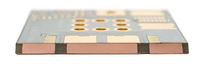
What is heavy copper pcb?
heavy copper pcb, as the name suggests, are PCB boards with thicker circuit layers. Some factories will distinguish PCB boards with circuit layer copper thickness ≥ 2oz from ordinary boards and call them thick copper boards. (There is currently no unified standard in the industry, but in the fourth edition of the “Electronic Circuit Industry Terms and Definitions” released by CPCA in 2021, the definition of thick copper plates is: containing line conductors with a copper thickness greater than 105 μm (3oz) Printed boards, including single-sided, double-sided and multi-layer boards).
GET PCB AND ASSEMBLY SERVICE QUOTE NOW!
Why do large currents require heavy copper pcbs?
First of all, heavy copper pcb have strong current carrying capacity.
According to the formula:
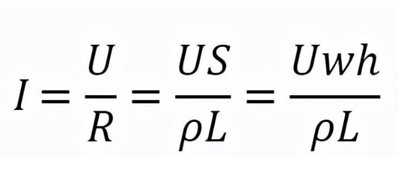
(Where, I represents the loadable current, U represents the voltage, R represents the resistance, S represents the line cross-sectional area, ρ represents the resistivity, L represents the line length, w represents the line width, h represents the line thickness)
It can be seen that when other conditions remain unchanged (especially the line width), the loadable current I of the line is proportional to the thickness h of the line. The thicker the line, the greater the loadable current.
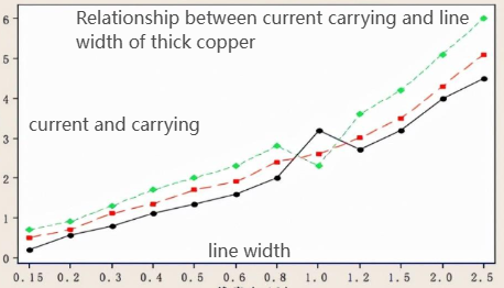
Correlation between current carrying, copper thickness and line width
Secondly, thick copper plates have good heat dissipation.
Everyone knows about metal substrates, the typical representatives of which are aluminum substrates and copper substrates, which have excellent heat dissipation properties. Thick copper plates, because the copper thickness is relatively thick, can also have certain heat dissipation properties.
The following is a set of related experiments on the impact of copper foil thickness on heat dissipation:
Using the single variable method, gradually increase the thickness of the copper foil and measure the temperature difference on both ends of the copper foil.
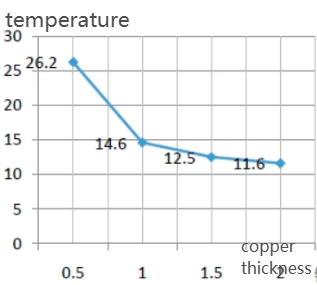
According to the change curve, it can be seen that as the thickness of the copper foil gradually increases, the temperature difference between the two end surfaces of the sample gradually decreases.
Therefore, designing the board into a heavy copper pcb can improve the heat dissipation performance of the board.
Finally, heavy copper pcb reduce thermal strain.
According to the formula:
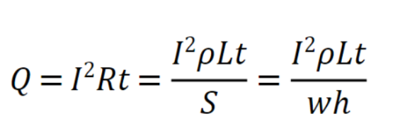
(Where, Q represents the calorific value, I represents the passing current, R represents the resistance, t represents the power-on time, ρ represents the resistivity, L represents the line length, S represents the line cross-sectional area, w represents the line width, and h represents the line thickness. )
It can be seen that, with other conditions remaining unchanged, the heat generated by the line is inversely proportional to the thickness of the line.
Therefore, designing the board as a heavy copper pcb can reduce the amount of heat generated, thereby reducing the thermal strain caused by heat generation.
To sum up, unlike ordinary PCBs, thick copper plates have the significant advantages of carrying large currents, good heat dissipation, and reducing thermal strain, which greatly reduces the risk of board burnout and is an excellent option for high-current PCB design. In addition, designing as a heavy copper pcb can also increase the mechanical strength of the circuit board and reduce the size of the end product.
With the development of science and technology, people need more and more electronic products with high performance, multiple functions, small size, capable of carrying large currents, and good heat dissipation. As a result, the demand for thick copper plates is also growing.
GET PCB MANUFACTURING AND ASSEMBLY QUOTE NOW!
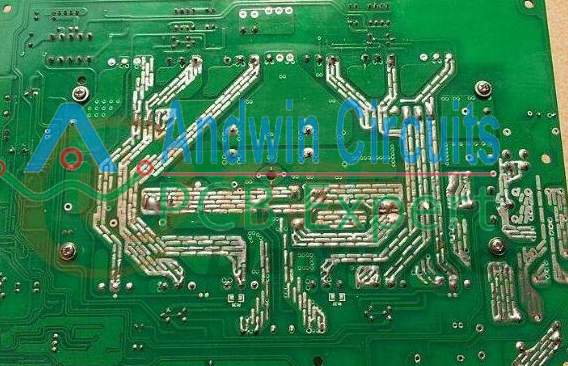
Heavy copper pcbs application areas
Having been deeply involved in the PCB field for many years, Andwin pcb has accumulated technology in the manufacturing of thick copper plates. After technological innovation and upgrades, it has supported the prototyping and mass production of thick copper plates, which can further meet the needs of our customers for PCBs.