Wiring tips for amplifier PCB
Join the exchange group
During the circuit design process, application engineers often overlook the layout of the printed circuit board (PCB). A common problem is that the circuit schematic is correct, but it does not work, or only operates at low performance. I will show you how to properly layout the circuit board of an op amp to ensure its functionality, performance, and robustness.
Recently, I worked with an intern on the OPA191 op amp in a non-inverting configuration with a gain of 2V/V, a load of 10kΩ, and a supply voltage of +/-15V. Figure 1 shows the schematic of the design.
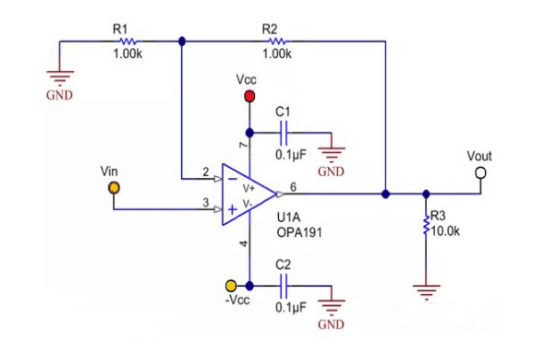
Figure 1: Schematic of OPA191 with non-inverting configuration OPA191 schematic
I asked the intern to layout the design, gave him general guidance on PCB layout (for example: minimize the trace path of the board, try to keep the components arranged closely to reduce the board space) ) space), and then let him design it himself. How difficult is the design process? It’s just a few resistors and capacitors, right? Figure 2 shows the layout of his initial attempt to design. The red line is the path to the top of the board, and the blue line is the path to the bottom.
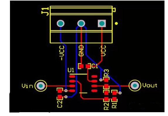
Figure 2: First layout attempt
Seeing his first layout attempt, I realized that the board layout was not as intuitive as I thought; I should have at least given him some more detailed guidance. He followed my advice exactly on the design: keeping the routing paths short and placing the parts close together. However, there is still much room for improvement in this layout to reduce the parasitic impedance of the board and optimize its performance.
The next step is to improve the layout. The first improvement we made was to move resistors R1 and R2 to the inverting pin (pin 2) of the OPA191; this helps reduce the stray capacitance of the inverting pin. The inverting pin of an op amp is a high impedance node and therefore highly sensitive. Long trace paths can act as a conductor to couple high-frequency noise into the signal chain. PCB capacitance at the inverting pin can cause stability issues. Therefore, the contact at the inverting pin should be as small as possible.
Moving R1 and R2 to pin 2 allows the load resistor R3 to be rotated 180 degrees, which allows the decoupling capacitor C1 to be closer to the positive supply pin (pin 7) of the OPA191. It is important to place the decoupling capacitors as close to the supply pins as possible. If the trace path between the decoupling capacitor and the power pin is long, the inductance of the power pin will increase, which will reduce performance.
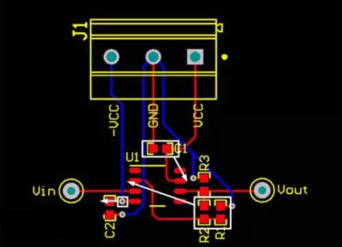
Figure 3: Improving the location of various parts of the layout
After moving the parts to the new location, you can still make some other improvements. You can widen the trace path to reduce the inductance, which is equivalent to the size of the pad to which the trace path connects. You can also prime the top and bottom ground planes of the board to create a reliable low-impedance path for the return current. Figure 4 shows our final layout.
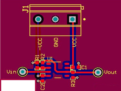
Figure 4: Final layout
Next time you lay out your printed circuit board, it is recommended that you follow the following layout conventions:
Try to minimize the number of connections to the inverting pin.
Place the decoupling capacitor as close to the power pin as possible.
If using multiple decoupling capacitors, place the smallest decoupling capacitor closest to the power pin.
Do not place vias between the decoupling capacitor and the power pin.
Extend the routing path as much as possible.
In the previous article, we talked about the correct layout of the instrumentation amplifier (op amp) PCB and provided a series of good layout practices for reference. Next, we will explore common mistakes when laying out an instrumentation amplifier (INA) and then show how to properly lay out an INA PCB.
INAs are used in applications where a differential voltage needs to be amplified, such as measuring the voltage across a shunt resistor in a high-side current sensing application. Figure 5 shows the schematic of a typical single-supply high-side current sensing circuit.
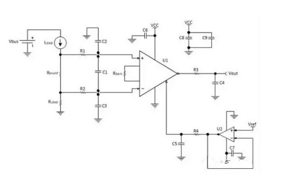
Figure 5: High-side current sensing schematic
Figure 5 measures the differential voltage across RSHUNT, R1, R2, C1, C2, and C3 are used to provide common-mode and differential-mode filtering, R3 and C4 provide output filtering for U1 INA, and U2 is used to buffer the INA reference pin. R4 and C5 are used to form a low-pass filter to minimize the noise introduced by the op amp to the INA reference pin.
While the schematic layout in Figure 5 looks intuitive, it is easy to make mistakes in the PCB layout, resulting in reduced circuit performance. Figure 6 shows three common mistakes that workers make when checking INA layouts.
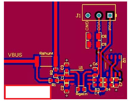
Figure 6: INA general PCB layout
As can be seen in the above figure, the first error is measuring the differential voltage Rshunt across the resistor. It can be seen that the Rshunt to R2 line is shorter, so its resistance is less than the Rshunt to R1 line resistance. This difference in line impedance can induce input bias current into the INA, resulting in a differential voltage on the U1 input side. Since the INA’s job is to amplify the differential voltage, unbalanced lines on the input side can cause errors. Therefore, it is necessary to ensure that the INA input lines are balanced and as short as possible.
The second error is related to the INA gain setting resistor, Rgain. The length from the U1 pin to the Rgain pad is longer than it should be, which creates additional resistance and capacitance. Since the gain is determined by the resistance between the INA’s gain setting pin, pin 1, and pin 8, the additional resistance can cause an error in the target gain. Since the INA’s gain setting pin is connected to the feedback section in the INA, the additional capacitance can cause stability issues. Therefore, ensure that the line connecting the gain setting resistor is as short as possible.
Then, the location of the buffer circuit reference pin may need to be improved. The reference pin buffer circuit is far away from the reference pin, which may increase the resistance of the reference pin, causing noise or other signals to couple into the line. The additional resistance at the reference pin may reduce the high common-mode rejection ratio (CMRR) provided by most INAs. Therefore, the reference pin buffer circuit should be placed as close to the INA reference pin as possible.
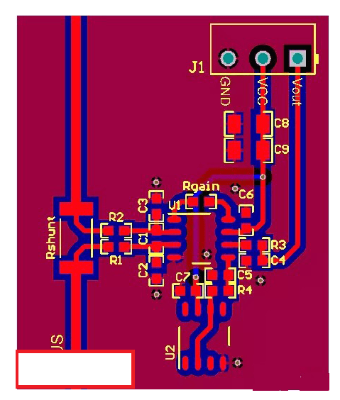
Figure 7 shows the layout after correcting these three errors.
In Figure 7, you can see that the wire lengths from R1 and R2 to the shunt resistors are the same and Kelvin connections are used. The gain setting resistors at the INA pins are as short as possible and the reference buffer circuit is as close to the reference pin as possible.
If you want to lay out a PCB for your INA in the future, be sure to follow these guidelines:
- Make sure all lines at the input are completely balanced;
Reduce line lengths and minimize capacitance on the gain setting pins;
Place the reference buffer circuit as close to the INA reference pin as possible;
- Place decoupling capacitors as close to the power pins as possible;
Cover at least one solid ground plane;
- Do not sacrifice a good layout for the use of silk screen for electronic components;
Follow the guidelines mentioned in the first part of this article