How to build flexible pcb
Understanding The Basics Of Flexible PCB Design
Understanding the basics of flexible PCB design is essential for anyone looking to delve into the world of modern electronics. Flexible printed circuit boards, or flexible PCBs, are a type of circuit board designed to bend and flex, offering a versatile alternative to traditional rigid PCBs. These boards are increasingly popular in applications where space constraints and mechanical flexibility are paramount, such as in wearable technology, medical devices, and complex electronic assemblies.
To begin with, it is crucial to understand the materials used in flexible PCB design.
Unlike rigid PCBs, which are typically made from fiberglass-reinforced epoxy laminate, flexible PCBs are constructed using flexible plastic substrates such as polyimide. Polyimide is favored for its excellent thermal stability, chemical resistance, and mechanical flexibility. This material allows the circuit board to bend and twist without damaging the conductive pathways, making it ideal for dynamic applications.
The design process of a flexible PCB starts with a clear understanding of the application’s requirements.
This involves determining the electrical, mechanical, and environmental constraints that the PCB must meet. For instance, the board’s thickness, bend radius, and the number of layers are critical factors that influence the design. A smaller bend radius allows for tighter bends, which is essential in compact devices. However, it is important to balance flexibility with durability, as excessive bending can lead to mechanical failure over time.
Once the requirements are established, the next step is to create a schematic diagram.
This diagram serves as a blueprint for the circuit, detailing the electrical connections and components. It is essential to use specialized software tools that cater to flexible PCB design, as they offer features that account for the unique properties of flexible materials. These tools help in optimizing the layout to minimize stress on the conductive traces during bending.
Transitioning from the schematic to the physical layout involves careful consideration of trace routing and component placement.
In flexible PCB design, trace routing must account for potential mechanical stress points. It is advisable to use curved traces instead of sharp angles, as this reduces stress concentration and enhances the board’s reliability. Additionally, components should be strategically placed to avoid areas of high flexing, thereby minimizing the risk of solder joint failure.
Another critical aspect of flexible PCB design is the selection of appropriate connectors and mounting techniques.
Flexible PCBs often require specialized connectors that can accommodate movement without compromising electrical integrity. Furthermore, mounting techniques such as adhesive bonding or encapsulation may be employed to secure the board within the device, providing additional mechanical support.
Testing and validation are the final steps in the design process.
Prototyping allows designers to evaluate the board’s performance under real-world conditions, ensuring that it meets all specified requirements. This phase may involve rigorous mechanical testing to assess the board’s flexibility and durability, as well as electrical testing to verify signal integrity and functionality.
In conclusion, understanding the basics of flexible PCB design involves a comprehensive approach that considers material selection, design requirements, schematic creation, layout optimization, and testing. By carefully addressing each of these elements, designers can create flexible PCBs that meet the demands of modern electronic applications, offering both reliability and versatility. As technology continues to evolve, the role of flexible PCBs is likely to expand, making them an integral component in the future of electronics design.
Essential Materials And Tools For Flexible PCB Fabrication
In the realm of modern electronics, flexible printed circuit boards (PCBs) have emerged as a pivotal component, offering versatility and adaptability in various applications. To embark on the journey of fabricating flexible PCBs, it is crucial to understand the essential materials and tools required for the process. This knowledge not only ensures the successful creation of these intricate circuits but also enhances the efficiency and reliability of the final product.
To begin with, the primary material used in flexible PCB fabrication is the substrate.
Unlike rigid PCBs, flexible PCBs utilize a flexible substrate, typically made from polyimide or polyester films. Polyimide is favored for its excellent thermal stability and mechanical properties, making it suitable for high-temperature applications. Polyester, on the other hand, is more cost-effective and is often used in applications where extreme thermal resistance is not a primary concern. The choice between these materials depends on the specific requirements of the project, such as flexibility, temperature resistance, and cost constraints.
In addition to the substrate, conductive materials are essential for creating the circuit paths on the flexible PCB.
Copper is the most commonly used conductive material due to its excellent electrical conductivity and ductility. It is typically deposited onto the substrate through processes such as electroplating or lamination. The thickness of the copper layer can vary depending on the current-carrying requirements of the circuit. Furthermore, to protect the copper traces and ensure their longevity, a solder mask is applied. This protective layer prevents oxidation and short circuits, thereby enhancing the durability of the PCB.
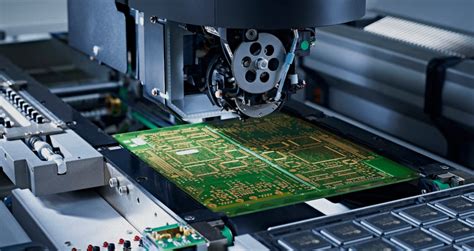
Moving on to the tools required for flexible PCB fabrication, precision and accuracy are paramount.
A laser cutting machine is often employed to cut the flexible substrate into the desired shape and size. This tool offers high precision, ensuring that the dimensions of the PCB are accurate and consistent. Additionally, a laminator is used to bond the copper foil to the substrate, creating a uniform and reliable conductive layer. The laminator must be capable of applying the appropriate pressure and temperature to achieve a strong bond without damaging the flexible substrate.
Moreover, a drilling machine is necessary for creating vias and holes in the PCB.
These holes are crucial for establishing electrical connections between different layers of the circuit. The drilling process must be meticulously controlled to prevent damage to the delicate substrate. Furthermore, an etching machine is used to remove excess copper from the board, leaving behind the desired circuit pattern. This process requires careful handling of chemicals and precise timing to ensure that the copper is etched accurately.
Finally, testing and inspection tools are indispensable in the fabrication process.
These tools, such as multimeters and automated optical inspection systems, are used to verify the electrical functionality and structural integrity of the flexible PCB. They help identify any defects or inconsistencies, allowing for timely corrections before the PCB is deployed in its intended application.
In conclusion, the fabrication of flexible PCBs necessitates a comprehensive understanding of the essential materials and tools involved. By selecting the appropriate substrate and conductive materials, and utilizing precise fabrication tools, one can create flexible PCBs that meet the demands of modern electronic applications. This meticulous approach not only ensures the functionality and reliability of the PCBs but also paves the way for innovation and advancement in the field of electronics.
Step-By-Step Guide To Designing A Flexible PCB Layout
Designing a flexible PCB layout requires a meticulous approach, as it involves several unique considerations compared to traditional rigid PCBs. The process begins with understanding the specific requirements of your project, which will guide the design choices you make. Initially, it is crucial to define the electrical and mechanical specifications, including the number of layers, the type of materials, and the overall dimensions of the flexible PCB. This foundational step ensures that the design will meet the necessary performance criteria and fit within the intended application.
Once the specifications are clear, the next step involves selecting the appropriate materials.
Flexible PCBs typically use polyimide as the substrate due to its excellent thermal stability and flexibility. The choice of copper thickness is also vital, as it affects the board’s flexibility and current-carrying capacity. Thinner copper layers enhance flexibility but may limit the current capacity, so a balance must be struck based on the application’s demands. Additionally, consider the use of coverlays or flexible solder masks to protect the circuitry while maintaining flexibility.
With materials selected, the design process moves to the schematic capture and layout design phase.
Using PCB design software, create a schematic that accurately represents the circuit. This schematic serves as a blueprint for the layout, ensuring that all components are correctly connected. During this phase, pay special attention to the placement of components and routing of traces. Flexible PCBs often require components to be placed in specific areas to accommodate bending and flexing. Therefore, it is essential to strategically position components to minimize stress on solder joints and traces.
As you transition to the layout design, consider the bend radius and flexing requirements.
The bend radius is a critical factor in flexible PCB design, as it determines how much the board can bend without damaging the traces or components. A larger bend radius generally reduces stress on the board, enhancing its durability. Additionally, when routing traces, aim to use curved traces instead of sharp angles, as this reduces stress concentrations and improves the board’s reliability.
Another important aspect is the stack-up configuration, which involves determining the arrangement of conductive and insulating layers.
The stack-up affects the board’s flexibility, impedance, and overall performance. For flexible PCBs, a symmetrical stack-up is often preferred to maintain uniform flexibility and prevent warping. Furthermore, consider using staggered vias instead of stacked vias to enhance mechanical reliability.
After completing the layout, it is essential to perform a thorough design rule check (DRC) to ensure that the design adheres to manufacturing constraints and industry standards.
This step helps identify potential issues such as trace width violations, spacing errors, or incorrect layer assignments. Addressing these issues early in the design process can prevent costly revisions later.
Finally, once the design is verified, generate the necessary files for manufacturing, including Gerber files, drill files, and a bill of materials (BOM).
These files provide the manufacturer with all the information needed to fabricate the flexible PCB. It is advisable to collaborate closely with the manufacturer to ensure that the design is feasible and to address any potential challenges that may arise during production.
In conclusion, designing a flexible PCB layout involves careful planning and attention to detail. By understanding the specific requirements, selecting appropriate materials, and following best practices in layout design, you can create a flexible PCB that meets the desired performance and reliability standards.
Common Challenges And Solutions In Flexible PCB Manufacturing
In the realm of electronics, flexible printed circuit boards (PCBs) have emerged as a pivotal innovation, offering a myriad of advantages over their rigid counterparts. However, the manufacturing of flexible PCBs is not without its challenges. Understanding these challenges and their corresponding solutions is crucial for ensuring the successful production of high-quality flexible PCBs.
One of the primary challenges in flexible PCB manufacturing is material selection.
Unlike rigid PCBs, which typically use FR-4 as a substrate, flexible PCBs require materials that can withstand bending and flexing. Polyimide is a common choice due to its excellent thermal stability and flexibility. However, selecting the right thickness and type of polyimide is essential to balance flexibility with mechanical strength. To address this, manufacturers often conduct thorough testing to determine the optimal material specifications for their specific applications.
Another significant challenge is the design complexity associated with flexible PCBs.
The need to accommodate bending and folding requires careful consideration of trace layout and component placement. Designers must ensure that traces are routed in a manner that minimizes stress during flexing, often employing curved traces instead of sharp angles. Additionally, components should be strategically placed to avoid areas of high mechanical stress. Advanced design software can aid in simulating the mechanical behavior of the PCB, allowing designers to make informed decisions and reduce the risk of failure.
The manufacturing process itself presents further challenges, particularly in terms of handling and processing the flexible materials.
Traditional PCB manufacturing equipment is often not suitable for flexible substrates, necessitating specialized machinery and techniques. For instance, during the etching process, flexible materials can be prone to stretching or tearing.
To mitigate this, manufacturers may use tension-controlled conveyors and employ gentler handling methods.
Furthermore, the lamination process must be carefully controlled to prevent air bubbles and ensure uniform adhesion, which is critical for maintaining the integrity of the flexible PCB.
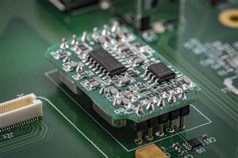
Soldering components onto flexible PCBs also poses unique challenges.
The heat from soldering can cause the flexible substrate to warp or deform, potentially leading to misalignment or damage. To overcome this, manufacturers often use low-temperature soldering techniques and employ fixtures to hold the PCB in place during the process. Additionally, the use of surface-mount technology (SMT) can help reduce the thermal stress on the PCB by minimizing the amount of heat required for component attachment.
Quality control is another area where challenges arise in flexible PCB manufacturing.
Due to their inherent flexibility, these PCBs are more susceptible to defects such as delamination, cracking, and warping. Implementing rigorous inspection protocols, including visual inspections and automated optical inspection (AOI) systems, is essential to identify and rectify defects early in the production process. Moreover, manufacturers may conduct flex testing to ensure that the PCB can withstand repeated bending without failure.
In conclusion, while the manufacturing of flexible PCBs presents several challenges, understanding these obstacles and implementing effective solutions can lead to the successful production of reliable and high-performance flexible circuits. By carefully selecting materials, optimizing design, employing specialized manufacturing techniques, and maintaining stringent quality control measures, manufacturers can overcome these challenges and fully leverage the benefits of flexible PCBs in a wide range of applications.