Issues to be noted when soldering PCB
After the copper clad laminate is processed to produce printed circuit graphics, various vias, and assembly holes, various components are assembled. After assembly, soldering is required to connect the components to the various circuits of the PCB. There are three types of soldering: wave soldering, reflow soldering, and manual soldering. The soldering connection of the components installed by the jack generally adopts wave soldering; the soldering connection of the surface mounted components generally adopts reflow soldering; individual devices and components are soldered by separate manual (electrochromium iron) due to the installation process requirements and individual repair soldering.
1.Solder resistance of copper clad laminate
As the substrate material of PCB, copper clad laminate is instantly exposed to high-temperature substances during soldering. Therefore, soldering is an important form of “thermal shock” for copper clad laminate and a test of its heat resistance. Ensuring the product quality of copper clad laminate in thermal shock is an important aspect of assessing the heat resistance of copper clad laminate. At the same time, the reliability of copper clad laminate during soldering is also related to its own pull-off strength, peel strength at high temperature, moisture and heat resistance and other performance indicators. In addition to the conventional solder resistance project, in recent years, in order to improve the reliability of copper clad laminate in soldering, some application performance measurement and assessment projects have been added. Such as moisture absorption and heat resistance test (treatment for 3 hours, then 260℃ soldering test), moisture absorption and reflow soldering test (placed at 30℃, relative humidity 70% for a specified time, reflow soldering test), etc. Copper clad laminate manufacturers should conduct strict solder resistance (also known as thermal shock blistering) tests according to standards before copper clad laminate products leave the factory. Printed circuit board manufacturers should also test this project in a timely manner after copper clad laminates enter the factory. At the same time, after a PCB sample is produced, the performance should be tested in small batches under simulated wave soldering conditions. Only after it is determined that the substrate meets the user’s requirements in terms of solder resistance can the PCB of this type be mass-produced and sent to the whole machine factory.
The determination method of solder resistance of copper clad laminate is basically the same as that of my country International (GBIT 4722-92), the US IPC standard (IPC-410 1), and the Japanese JIS standard (JIS-C-6481-1996). The main requirements are:
① The arbitration determination method is the “floating solder method” (the sample floats on the solder surface);
② The sample size is 25 mm X 25 mm;
③ If a mercury thermometer is used for the temperature measurement point, it means that the parallel position of the mercury head and tail in the solder is (25 ± 1) mm; the IPC standard is 25.4 mm;
④ The depth of the solder bath is not less than 40 mm.
It should be noted that the temperature measurement position has a very important influence on the correct and true reflection of the solder resistance level of a board. Generally, the heat source for solder heating is at the bottom of the tin bath. The greater the distance (the deeper) from the temperature measurement point to the solder liquid surface, the greater the deviation between the temperature of the solder liquid and the measured temperature. At this time, the lower the liquid surface temperature is than the measured temperature, the longer the blistering time of the board with resistance to dip soldering measured by the sample floating soldering method will be.
2. Wave soldering process
In wave soldering process, the welding temperature is actually the temperature of solder, which is related to the type of soldering. The welding temperature should generally be controlled below 250’c. Too low welding temperature affects the quality of welding. As the welding temperature increases, the dip soldering time is relatively significantly shortened. Too high welding temperature will cause blistering, delamination of the circuit (copper cylinder) or substrate, and serious warping of the board. Therefore, the welding temperature must be strictly controlled.
3. Reflow soldering process
Generally, the temperature of reflow soldering is slightly lower than the wave soldering temperature. The setting of reflow soldering temperature is related to the following aspects:
① Type of reflow soldering equipment;
② Setting conditions such as line speed;
③ Type and thickness of substrate material;
④ Size of PCB, etc.
The setting temperature of reflow soldering is different from the surface temperature of PCB. At the same reflow soldering set temperature, the PCB surface temperature is different due to the different types and thicknesses of substrate materials (see Figures 1 and 2).
During the reflow soldering process, the heat resistance limit of the substrate surface temperature where the copper foil bulges (blistering) occurs will change with the preheating temperature of the PCB and whether there is moisture absorption. As can be seen from Figure 3, the lower the preheating temperature of the PCB (the surface temperature of the substrate), the lower the heat resistance limit of the substrate surface temperature where the bulging problem occurs. Under the conditions of constant reflow soldering set temperature and reflow soldering preheating temperature, the surface temperature drops due to moisture absorption of the substrate.
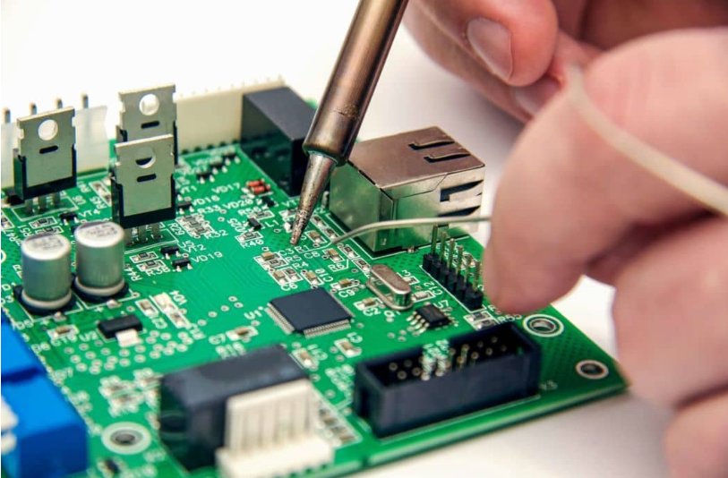
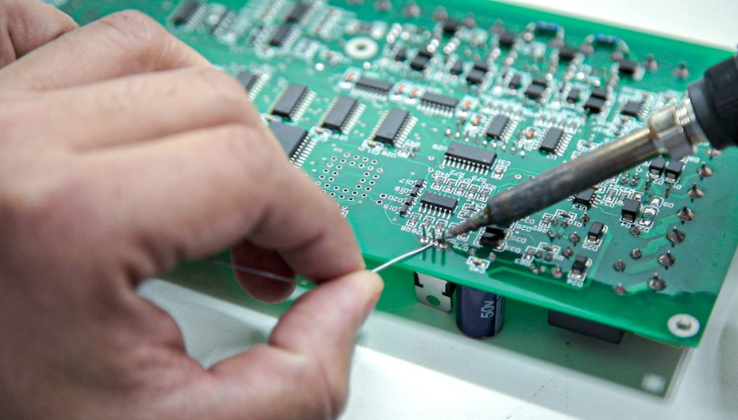
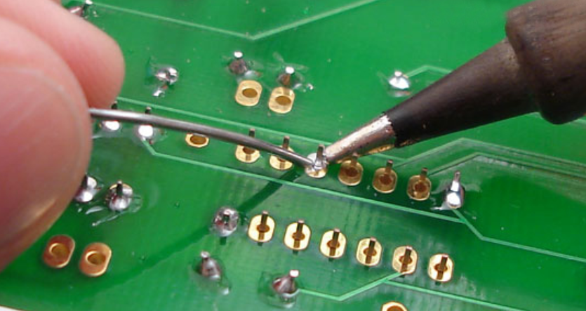
4. Manual welding processing
When repairing soldering or performing separate manual soldering on special components, the surface temperature of the electrochromium iron is required to be below 260℃ for paper-based copper-clad laminates and below 300℃ for glass-fiber cloth-based copper-clad laminates. And try to shorten the welding time, generally requiring; less than 3s for paper substrates and less than 5s for glass-fiber cloth substrates.