
PCB DFM Checklist: 20 Points to Review Before Manufacturing
Manufacturing a PCB without proper Design for Manufacturing (DFM) review is like sending Gerber files into a black box—you’ll only discover what went wrong after boards arrive defective. Industry data shows systematic DFM checks cut rework rates by over 40%, because catching issues at design stage costs a fraction of what you’ll pay for board respins.
This checklist covers 20 verification points that separate boards fabricating cleanly on the first pass from those triggering engineering queries, yield losses, or manufacturing failures.
Why DFM Review Matters
A board can pass every design rule check and still fail on the manufacturing floor. DRC engines validate your layout against configured rules, but they don’t know your fabricator’s actual process limits or assembler’s pick-and-place clearances. DFM review closes that gap by verifying your design against physical constraints of real manufacturing equipment.
The cost of fixing design flaws grows roughly 10× at each stage: a trace spacing issue corrected in layout costs 30 minutes; the same issue during CAM costs hours; catching it after fabrication means scrapping boards and paying for a respin.

Fabrication Design Rules
1. Trace Width and Spacing
Standard process limits are 4 mil (0.1mm) trace/space, but pushing these limits increases cost and reduces yield. For high-reliability designs, maintain 6 mil (0.15mm) or wider. Check dense areas like BGAs where autorouters often violate spacing rules.
2. Annular Ring Size
IPC-6012 Class 2 requires minimum 2 mil (0.05mm) annular ring, but this leaves no margin. Use 4 mil (0.1mm) minimum—preferably 5-6 mil for internal layers. Inadequate annular rings cause via failures: breakout, tangency, or intermittent connections.
3. Drill Sizes and Aspect Ratio
Confirm drill sizes fall within 8 mil (0.2mm) to 250 mil (6.35mm) range. Critical is aspect ratio: board thickness divided by drill diameter. Standard processes handle 10:1; exceeding this requires specialized drilling. A 0.012″ hole in 0.125″ board is 10.4:1 and may be rejected.
4. Copper Balance
Aim for 40-60% copper coverage across each layer. Heavily imbalanced layers cause warping during lamination. Add copper pour or hatched fills to empty areas, especially on outer layers and power planes.
5. Solder Mask Clearance
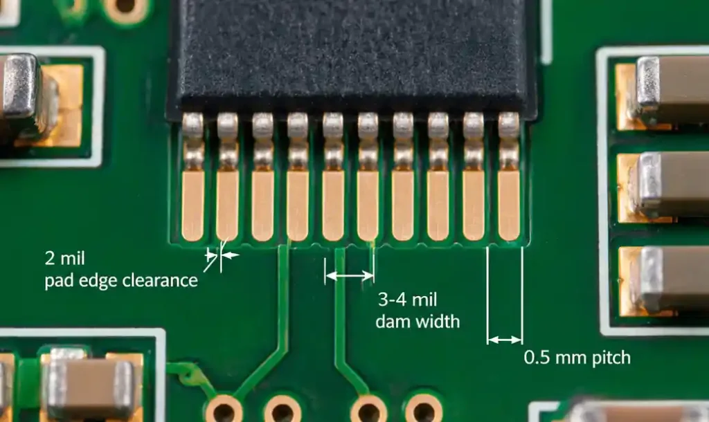
Standard clearance is 2 mil (0.05mm) beyond pad edge, with 3-4 mil (0.075-0.1mm) minimum dam between pads. Fine-pitch components (0.5mm or tighter) often require solder mask defined pads (SMD) where mask opening is smaller than copper pad.
6. Silkscreen Legibility
Use 50 mil height and 7-8 mil stroke for production readability. Verify silkscreen doesn’t overlap pads, vias, or mask openings—most fabricators will clip overlapping text without notification.
7. Board Outline and Dimensions
Board outline must be a closed, continuous path on a dedicated mechanical layer. PCB fabrication tolerance is typically ±0.005″ (0.13mm), and slots or mounting holes have ±0.003″ (0.075mm) positional tolerance.
8. Layer Stackup Documentation
Provide complete stackup specification: layer count, copper weight, dielectric material (FR-4 standard Tg, high-Tg, Rogers), and final board thickness. For impedance-controlled designs, specify target impedance (e.g., 50Ω ±10%).
Assembly Design Rules
9. Component Clearance
Minimum body-to-body clearance is 20 mil (0.5mm) for automated assembly, but 40 mil (1mm) is preferred. Tall components need 100 mil (2.54mm) or more clearance. Insufficient clearance causes placement errors or makes rework impossible.

10. Pad Dimensions and Footprints
Footprints must match IPC-7351 standards for the actual component package. Verify against manufacturer’s datasheet, especially for fine-pitch ICs. For leadless parts (QFN, DFN, LGA), paste stencil apertures typically need reducing to 80-90% of pad size to prevent bridging.
11. Fiducial Marks
Place at least three global fiducials near board corners for pick-and-place calibration. Use 1mm diameter bare copper circles with 2mm clearance. For fine-pitch devices (0.4mm pitch or tighter), add local fiducials within 5mm of the component.
12. Thermal Relief for Through-Hole Parts
Through-hole pads connecting to large copper pours need thermal relief—spokes that thermally isolate the pad while maintaining electrical connection. Use 4 spokes at 90° with 10-15 mil (0.25-0.4mm) width.
13. Panelization Requirements
If ordering as arrays, specify tooling holes, breakaway method (V-scoring, mouse bites, or tab routing), and edge clearance. Learn more about panelization strategies to optimize cost. Leave 5mm minimum between board edge and components.
14. Polarity and Pin 1 Indicators
Mark polarity on both silkscreen and assembly drawing for diodes, electrolytic capacitors, and ICs. Use consistent conventions: dot for pin 1, plus symbol for positive terminal. Add polarity to assembly drawing as backup.

Test and Inspection Points
15. Test Point Accessibility
Flying probe test requires accessible test points. Test pads should be 40 mil (1mm) diameter minimum with 100 mil (2.54mm) center-to-center spacing. Maintain 100 mil clearance around test points.
16. Electrical Test Net Coverage
Ensure critical nets have accessible test points: power rails, ground, key signals. Buried vias and vias under components can’t be probed. Flying probe testing can reach most exposed pads, but it’s slower and can’t detect shorts between internal layers.
Special Considerations
17. Controlled Impedance Routing
For high-speed signals (USB, PCIe, DDR, RF), verify trace geometry matches your impedance target. Calculate impedance using your fabricator’s stackup dielectric constants—FR-4 Dk varies from 4.2 to 4.5. Request impedance testing coupons for TDR verification.
18. Via-in-Pad Design
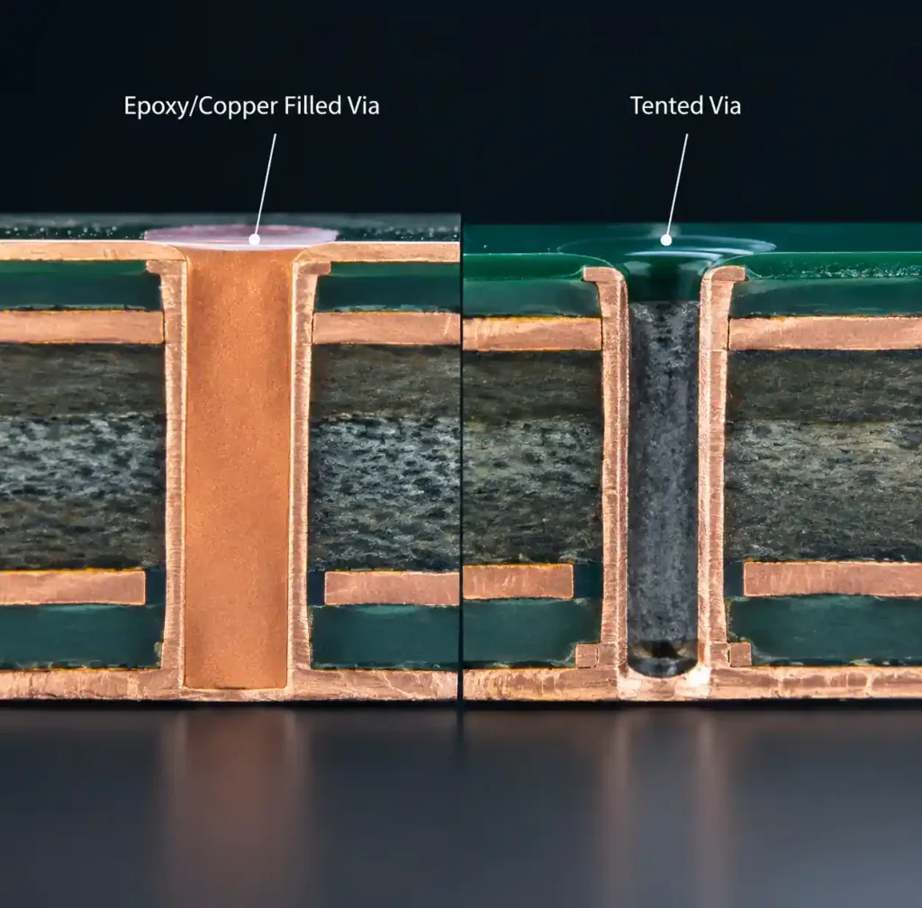
Placing vias inside BGA or QFN pads improves routing density but requires via plugging or tenting to prevent solder wicking. Plugged vias (filled with epoxy or copper) cost more but allow normal assembly.
19. Component Availability
Check lead times for all parts before committing to manufacturing. Parts listed as “active” can go to backorder between design and production. Long-lead components (6-12 weeks) gate your entire build if not procured in advance.
20. Design File Checklist
Verify you’re providing: Gerber files (all copper layers, solder mask, silkscreen, paste mask, board outline), drill files, fabrication drawing with stackup, BOM with manufacturer part numbers, centroid file, and assembly drawing. Missing files cause fab holds and quote delays.
Common DFM Violations by Category
| Violation Type | Typical Causes | Impact | Prevention |
|---|---|---|---|
| Insufficient annular ring | Tight drill-to-pad clearance, registration variation | Via failures, intermittent connections | 4 mil minimum ring, 5-6 mil for internal layers |
| Trace/space violations | Auto-router minimum settings, dense routing | Shorts, opens, yield loss | 6 mil trace/space for standard fabrication |
| Missing thermal relief | Direct connection to planes | Soldering defects, cold joints | 4-spoke relief, 10-15 mil spokes |
| Component clearance | Dense placement, cost optimization | Assembly errors, no rework access | 40 mil body-to-body minimum |
| Inadequate fiducials | Missing or poorly placed | Placement errors on fine-pitch parts | 3 global + local for fine-pitch devices |
DFM Check Timing and Ownership
| Stage | Responsibility | Actions | Tools |
|---|---|---|---|
| Pre-layout | Designer | Review fab capabilities, select design rules | Capability tables, fab house specs |
| During layout | Designer | DRC checks, visual inspection | EDA DRC engine |
| Pre-release | Designer + Team | Full checklist review, generate files | Checklist, Gerber viewer |
| Post-submission | Fab/Assembly | CAM review, DFM report generation | CAM software, automated DFM tools |
Run DFM review twice: once before layout starts (to catch capability mismatches early) and again before releasing files to manufacturing. The earlier you catch issues, the cheaper they are to fix.

Handling Fab House DFM Reports
Most PCB manufacturers run automated DFM checks and send reports highlighting potential issues. Review every flagged item—some are false positives, but many are legitimate issues that will cause yield loss.
Respond to fab queries promptly. “Proceed as-is” means you accept the risk; “revise and resubmit” delays your schedule but ensures a manufacturable board.
Frequently Asked Questions
What’s the difference between DFM and DFT?
DFM (Design for Manufacturing) ensures your board can be fabricated and assembled without defects. DFT (Design for Test) ensures the finished board can be tested effectively. DFM focuses on trace widths and clearances; DFT focuses on test point access.
How do I know my fabricator’s actual capabilities?
Request a capability table—reputable fabricators publish detailed specifications including minimum trace/space, drill sizes, layer counts, and tolerance limits. Match your design to their standard capabilities to avoid premium pricing.
Should I use my EDA tool’s built-in DFM checker?
EDA DFM checkers catch basic violations but don’t replace a full review. They don’t know your specific fabricator’s limits or assembly house equipment. Use EDA DFM as a first pass, then review manually.
Can I skip DFM review for simple two-layer boards?
Even simple boards benefit from DFM review. A two-layer board with inadequate annular rings or missing fiducials still fails in manufacturing. The review takes 20-30 minutes and prevents delays worth days or weeks.
What’s the typical cost of a board respin?
Board respins cost 2-4 weeks and $500-$5,000+ depending on complexity. Assembly delays from DFM issues cost even more if you’re blocking production. One DFM review pays for itself by preventing a single respin.
How do I handle high-density designs that violate standard rules?
High-density designs (HDI, fine-pitch BGAs) require advanced fabrication processes with tighter tolerances and higher cost. Work with your fabricator early to understand their HDI capabilities: laser-drilled microvias, sequential lamination, and impedance control limits.
Conclusion
DFM review is not a formality—it’s the difference between boards that work on the first build and those that trigger expensive respins or assembly failures. The 20 points in this checklist address the most common manufacturing violations: insufficient annular rings, spacing violations, missing fiducials, inadequate component clearance, and incomplete file sets. Run through this checklist before you release files. It takes 30 minutes and catches issues that cost weeks to fix after fabrication starts. Work with your fabricator and assembler as partners—share your design constraints early, ask questions about capabilities, and respond to DFM reports promptly.