
PCB Design for Mass Production: 10 DFM Rules to Reduce Cost and Improve Yield
Manufacturing defects cause 40% of product delays in electronics production, with design-related issues accounting for the majority of rework. When scaling from prototype to mass production of 10,000+ units, design for manufacturability (DFM) principles become the difference between 92% yield and 98% yield—translating to thousands of dollars in scrap reduction alone.

What is DFM and Why It Matters for Mass Production
Design for Manufacturability optimizes PCB layouts to align with factory capabilities, reducing fabrication errors and assembly defects before production begins. Unlike prototyping where 1-2 respins are acceptable, mass production demands first-pass success. A single DFM oversight—undersized annular rings, tight component spacing, or poor panelization—can reduce yield by 5-15% across thousands of units.
Real factory data shows properly implemented DFM reduces unit cost by 20-40% while improving yield from industry average 92% to 97-99%. This guide presents 10 practical rules validated across automotive, industrial, and consumer electronics production.
Rule 1: Use Standard Material Specifications
Custom materials increase cost and lead time. Standard FR-4 with Tg 130-140°C, 1.6mm thickness, and 1 oz copper covers 80% of applications. Requesting exotic materials like Rogers or polyimide for non-RF designs adds 3-5 days lead time and 40-60% cost premium.
Material selection should match operating requirements: FR-4 handles -40°C to +85°C reliably. High-Tg (170-180°C) becomes necessary only when sustained temperatures exceed 130°C, such as automotive PCB under-hood applications or industrial motor drives.
For copper weight, 1-2 oz suffices for signal layers and power traces up to 5-10A. Heavy copper (4-6 oz) is required only for power electronics above 15A, where trace width calculations justify the added cost.
| Material Specification | Standard (Low Cost) | Custom (Premium) | Typical Cost Impact |
|---|---|---|---|
| Base Material | FR-4 Tg 130-140°C | Rogers, Polyimide, Ceramic | +40-120% |
| Board Thickness | 1.6 mm (63 mil) | 0.8 mm, 2.0 mm, 2.4 mm | +15-35% |
| Copper Weight | 1 oz (35 μm) | 2 oz, 4 oz, 6 oz | +20-80% |
| Surface Finish | HASL, ENIG | Immersion Silver, OSP, ENEPIG | +10-50% |
Rule 2: Optimize Layer Count
Adding layers increases cost exponentially. A 4-layer board costs 2-3× more than 2-layer; 6-layer costs 3-5× more. During mass production, this multiplies across every unit. Before defaulting to 6 layers, verify routing density actually requires it.
Modern design tools enable higher density with proper via strategy. HDI techniques like blind and buried vias allow more routing in fewer layers, but only make economic sense above 5,000-10,000 units where NRE cost amortizes.
For typical designs: 2 layers handle simple single-sided component layouts; 4 layers accommodate moderate complexity with ground/power planes; 6+ layers are necessary only for high pin-count BGAs, DDR routing, or impedance-critical designs above 1 GHz.
Rule 3: Maximize Panel Utilization
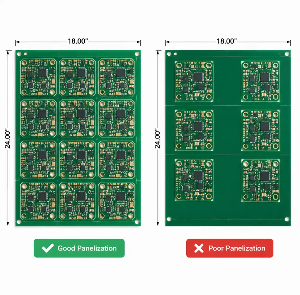
Panel utilization directly impacts per-unit cost. Standard panel sizes are 18×24 inches (457×610 mm). A poorly panelized 80×100 mm board might fit only 8-10 pieces per panel (70% utilization), while optimized layout fits 12-15 pieces (85-90% utilization)—reducing cost by 20-30%.
Calculate array configuration before finalizing board outline. Allow 5mm spacing between boards for V-scoring or 3mm for tab routing. Add tooling holes at panel corners and fiducial marks for automated assembly registration.
Consider depaneling method during design: V-scoring requires straight lines with no internal cutouts; mouse bites handle irregular shapes but leave rough edges; tab routing offers cleanest separation but adds 2-3 days to lead time.
Rule 4: Standardize Via Sizes and Spacing
Using multiple via sizes increases drill hit count and tooling changes. Limit designs to 2-3 via sizes maximum. Standard 12 mil (0.3 mm) finished hole with 24 mil (0.6 mm) pad handles signal vias; 16-20 mil holes for power/ground connections.
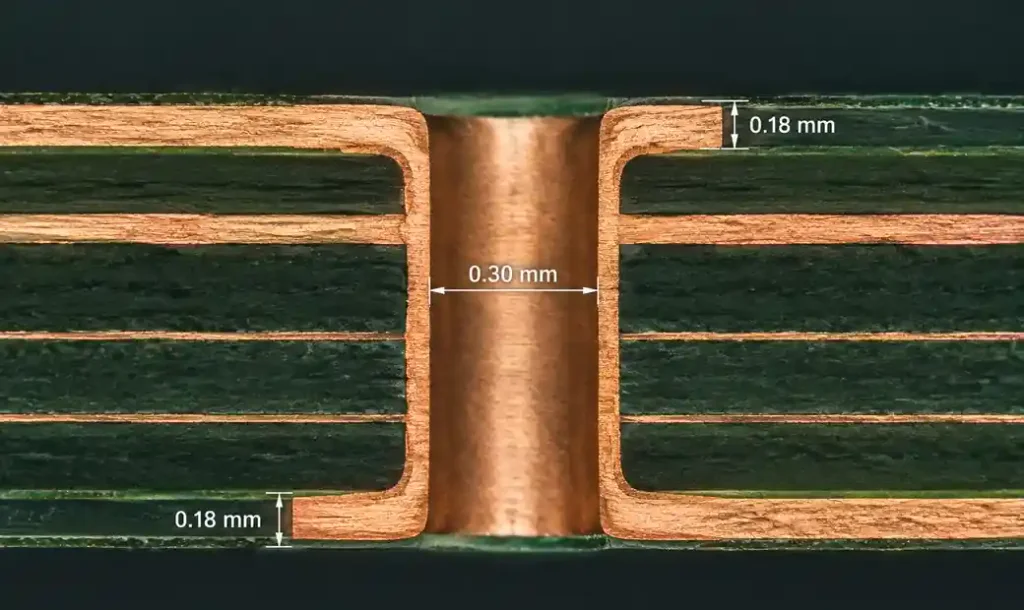
Maintain minimum 8 mil annular ring (pad edge to hole edge) for standard processes. Smaller rings risk breakout during drilling, especially in multilayer boards where registration tolerance accumulates. IPC-6012 Class 2 requires 4 mil minimum, but conservative designs use 6-8 mil for 95%+ yield.
Via-in-pad designs require special processing—resin plugging and planarization add $50-150 NRE cost plus $5-15 per panel. Reserve via-in-pad for dense BGA fanouts where escape routing is impossible, not convenience.
Rule 5: Maintain Manufacturing-Compatible Trace Width and Spacing
Trace width and spacing capabilities vary by fabricator class. Standard 6/6 mil (0.15 mm) trace/space covers general designs with margin. Pushing to 4/4 mil or 3/3 mil increases cost 25-40% and reduces yield due to etching variation.
Before specifying tight geometries, verify actual need. A 50Ω controlled impedance line on 1.6mm FR-4 with 1 oz copper requires only 10-12 mil width—well within standard capability. Similarly, high-speed differential pairs rarely need spacing below 5 mil when using proper layer stackup design.
Design trace widths with 20-30% margin above calculated minimum. This accommodates manufacturing tolerance and copper undercutting during etching, maintaining impedance within ±10% target.
| Trace/Space Capability | Manufacturing Class | Typical Yield | Cost Factor |
|---|---|---|---|
| 8/8 mil (0.20 mm) | Standard | 98-99% | 1.0× (baseline) |
| 6/6 mil (0.15 mm) | Standard+ | 96-98% | 1.1-1.2× |
| 4/4 mil (0.10 mm) | Advanced | 92-95% | 1.4-1.6× |
| 3/3 mil (0.075 mm) | Premium | 88-92% | 1.8-2.2× |
Rule 6: Use Standard Components and Packages
Component selection impacts assembly cost more than BOM price alone. Standard packages (0805, 0603, SOT-23, SOIC) have lower placement cost and higher availability than exotic parts. Pick-and-place machines handle 0402 and larger without vision system adjustments.
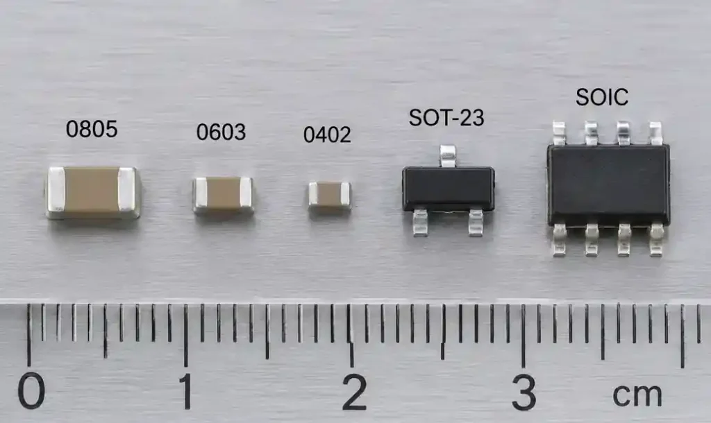
Avoid mixing imperial and metric packages unnecessarily. Choose either 0603 (imperial) or 1608 (metric), not both for identical value resistors. Consolidating passive component sizes reduces feeder setup time—on high-volume lines, this saves 15-30 seconds per board.
BGA packages require X-ray inspection, adding $0.50-2.00 per board in testing cost. Use QFN packages where possible—they offer similar thermal performance with AOI-compatible inspection. When BGAs are necessary, maintain minimum 0.5mm pitch and follow IPC-7351 land pattern guidelines.
For production above 5,000 units, specify components with multiple approved manufacturers (AVL with 2-3 sources). Single-source parts risk production stops if supply constrained. Verify all components have >90 day inventory lead time before design freeze.
Rule 7: Implement Proper Test Point Strategy
Test points enable automated testing but consume board space. Place test points on 100 mil (2.54 mm) or 50 mil (1.27 mm) grid for standard ICT fixtures. Flying probe requires no fixture but costs $2-5 per board—economical only below 500 units.

ICT provides 95-98% fault coverage at $0.20-0.80 per board after fixture amortization. Design 40-50 mil diameter test points with minimum 3 mil clearance for probe contact. Avoid placing under components or near board edges (maintain 200 mil keepout).
For mass production, combine ICT with functional testing for 99%+ defect detection while minimizing PCBA testing cost.
Rule 8: Add Fiducial Marks for Assembly
Fiducial marks are essential for automated SMT placement accuracy. Use 1mm diameter bare copper circles in soldermask-free clearings. Place global fiducials (3 minimum) at panel corners and local fiducials near fine-pitch components (≤0.5mm pitch).
Fiducials must be non-functional—dedicated marks, not component pads or vias. Position them at non-collinear locations to enable rotational alignment. For two-sided assembly, add fiducials to both sides.
IPC-7351 specifies 2× fiducial diameter soldermask opening and 3× copper-free clearance around each mark. This ensures vision system accuracy to ±25 microns, necessary for 0201 components and 0.4mm pitch BGAs.
Rule 9: Complete Documentation Package
Incomplete documentation causes production delays and misinterpretation. Provide Gerber RS-274X files (not just Gerber X2), IPC-356 netlist, BOM with manufacturer part numbers, and assembly drawings showing component polarity and orientation.
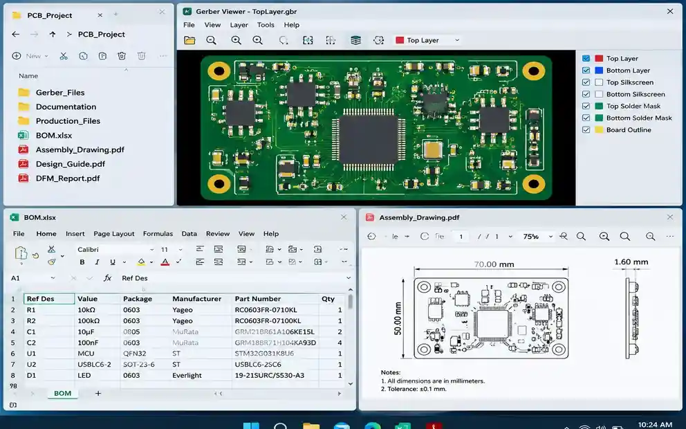
Include fabrication notes specifying: board material and Tg, copper weight per layer, surface finish, impedance requirements with tolerances, and any special processes (edge plating, blind vias, controlled depth drilling). Export Gerbers at 4.6 resolution (6 decimal places) to maintain ±0.1 mil accuracy.
For assembly, provide pick-and-place centroid file in ASCII CSV format with clear column headers (Designator, X, Y, Rotation, Layer). Verify rotation angles match your PCB assembly vendor’s convention—0° or 270° for horizontal components.
Rule 10: Match Supplier Capabilities Before Design Freeze
Running DFM analysis after layout completion wastes time. Review target manufacturer’s capability table during schematic design to set achievable constraints. Key parameters: minimum hole size, aspect ratio limit, trace/space capability, registration accuracy, and impedance tolerance.
Request preliminary DFM review at 80% layout completion—before routing finalization. This catches issues like impossible via structures, tight clearances, or copper balance problems while changes are still efficient. Most PCB manufacturers provide free DFM analysis for production orders.
Submit stackup for approval before starting layout. Confirm layer arrangement, impedance calculations, and material selections match fabricator’s standard offerings. Custom stackups add 3-7 days lead time and 15-30% cost.
DFM Impact on Total Cost of Ownership
DFM optimization delivers substantial cost savings through yield improvement. A 4% yield gain on 10,000 units prevents 400 scrap boards, saving $6,000-16,000 per run at typical manufacturing costs.
| Production Volume | Poor DFM (92% Yield) | Good DFM (98% Yield) | Cost Savings |
|---|---|---|---|
| 1,000 units | 80 scrap boards | 20 scrap boards | $900-2,400 |
| 10,000 units | 800 scrap boards | 200 scrap boards | $9,000-24,000 |
| 100,000 units | 8,000 scrap boards | 2,000 scrap boards | $90,000-240,000 |
| 500,000 units | 40,000 scrap boards | 10,000 scrap boards | $450,000-1.2M |
Frequently Asked Questions
When should I start DFM review in the design cycle?
Begin during schematic design by selecting standard components. Conduct formal review at 80% layout completion, before final routing adjustments.
What’s the minimum production volume where DFM becomes critical?
DFM applies to all volumes, but ROI becomes substantial above 1,000 units. Above 5,000 units, comprehensive review justifies dedicated engineering time.
How do I balance DFM with performance requirements?
Performance takes precedence—DFM optimizes how you meet requirements. If 4/4 mil traces are necessary for impedance control, use them but minimize their extent.
Can automated DFM tools replace manual review?
No. Automated checks catch rule violations but miss context issues like poor panelization or component consolidation. Combine both approaches.
What documentation format do manufacturers prefer?
Gerber RS-274X for fabrication, CSV centroid file for assembly, BOM with manufacturer part numbers, and assembly drawing PDF showing polarity.
Conclusion
Implementing these 10 DFM rules reduces PCB manufacturing cost by 20-40% and improves yield from 92% to 98%+ in mass production. The highest-impact rules are panel utilization (20-30% cost reduction), component standardization (15-25% assembly cost savings), and via/trace standardization (10-20% fabrication cost reduction). Together, these deliver majority DFM benefits with minimal design effort. Build DFM reviews into your development process at schematic, layout, and pre-production stages for consistent results.