Non flex cut pcb
Understanding Non Flex Cut PCB: Design and Applications
Printed Circuit Boards (PCBs) are the backbone of modern electronic devices, providing the necessary platform for mounting and interconnecting various electronic components. Among the different types of PCBs, non-flex cut PCBs hold a significant place due to their unique design and applications. Understanding the intricacies of non-flex cut PCBs requires a closer examination of their structure, manufacturing process, and the specific scenarios in which they are most effectively utilized.
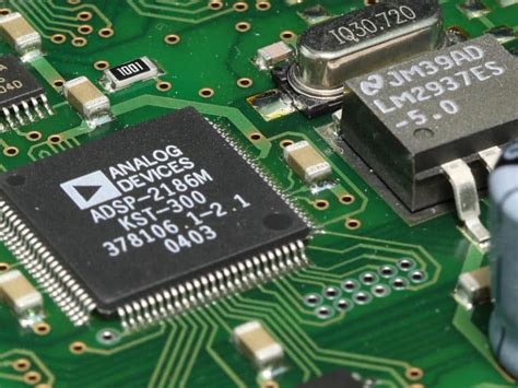
Non-flex cut PCBs, as the name suggests, are rigid circuit boards that do not incorporate flexible sections.
Unlike their flexible counterparts, these PCBs are designed to maintain a fixed shape, providing a stable and durable platform for electronic components. The rigidity of non-flex cut PCBs is achieved through the use of solid substrates, typically made from materials such as fiberglass-reinforced epoxy resin, commonly known as FR-4. This material is favored for its excellent mechanical strength, thermal resistance, and electrical insulation properties, making it ideal for a wide range of electronic applications.
The design process of non-flex cut PCBs involves several critical steps, beginning with the creation of a schematic diagram that outlines the electrical connections and component placements.
This is followed by the layout design, where the physical arrangement of the components and the routing of electrical traces are meticulously planned. Advanced software tools are often employed to optimize the layout, ensuring minimal signal interference and efficient use of space. Once the design is finalized, the manufacturing process commences, involving the etching of copper layers to form the desired circuit patterns, drilling of holes for component leads, and the application of solder masks to protect the circuitry.
Non-flex cut PCBs are particularly advantageous in applications where mechanical stability and reliability are paramount.
For instance, they are extensively used in consumer electronics such as televisions, computers, and smartphones, where the rigid structure provides a robust foundation for complex circuitry. Additionally, these PCBs are prevalent in industrial and automotive sectors, where they must withstand harsh environmental conditions and mechanical stresses. The rigidity of non-flex cut PCBs ensures that they can endure vibrations, shocks, and temperature fluctuations without compromising performance.
Moreover, non-flex cut PCBs are often preferred in high-frequency applications due to their ability to maintain signal integrity.
The stable substrate minimizes signal loss and electromagnetic interference, which is crucial in telecommunications and networking equipment. Furthermore, the cost-effectiveness of non-flex cut PCBs makes them an attractive option for mass production, as they can be manufactured efficiently and at a lower cost compared to flexible or rigid-flex PCBs.
In conclusion, non-flex cut PCBs play a vital role in the electronics industry, offering a reliable and cost-effective solution for a wide array of applications. Their rigid design, coupled with excellent mechanical and electrical properties, makes them indispensable in scenarios where stability and performance are critical. As technology continues to advance, the demand for non-flex cut PCBs is expected to grow, driven by the need for durable and efficient electronic solutions. Understanding the design and applications of these PCBs is essential for engineers and manufacturers seeking to harness their full potential in the ever-evolving landscape of electronic devices.

Advantages and Limitations of Non-Flex Cut PCB in Modern Electronics
In the rapidly evolving landscape of modern electronics, the choice of printed circuit board (PCB) design plays a crucial role in determining the performance, reliability, and cost-effectiveness of electronic devices. Among the various types of PCBs, non-flex cut PCBs have garnered attention for their distinct advantages and limitations. Understanding these characteristics is essential for engineers and designers who aim to optimize their electronic products.
One of the primary advantages of non-flex cut PCBs is their structural integrity.
Unlike their flexible counterparts, non-flex cut PCBs are rigid, providing a stable platform for mounting components. This rigidity ensures that the components remain securely in place, reducing the risk of mechanical failure due to vibrations or physical stress. Consequently, non-flex cut PCBs are particularly well-suited for applications where durability and stability are paramount, such as in industrial machinery, automotive systems, and consumer electronics that are subject to frequent handling.
Moreover, non-flex cut PCBs offer a cost-effective solution for many electronic applications.
The manufacturing process for these PCBs is generally simpler and less expensive than that for flexible PCBs. This is because non-flex cut PCBs do not require the specialized materials and processes needed to produce flexible circuits. As a result, they are an attractive option for projects with budget constraints or for mass production scenarios where cost efficiency is a priority.
In addition to cost benefits, non-flex cut PCBs provide excellent electrical performance.
The rigid nature of these boards allows for precise control over the layout and spacing of conductive traces, which can minimize signal interference and improve overall circuit performance. This precision is particularly beneficial in high-frequency applications where signal integrity is critical. Furthermore, the thermal management capabilities of non-flex cut PCBs are often superior to those of flexible PCBs, as the rigid substrate can better dissipate heat generated by electronic components.
Despite these advantages, non-flex cut PCBs are not without their limitations.
One significant drawback is their lack of flexibility, which can be a disadvantage in applications that require the PCB to conform to complex shapes or fit into tight spaces. This rigidity can also pose challenges during the assembly process, as non-flex cut PCBs cannot be bent or twisted to accommodate design constraints. Consequently, designers must carefully consider the physical layout of the device and ensure that the PCB can be integrated without compromising the overall design.
Another limitation of non-flex cut PCBs is their susceptibility to mechanical stress.
While their rigidity provides stability, it also makes them more prone to cracking or breaking under excessive force. This vulnerability necessitates careful handling during manufacturing and assembly to prevent damage. Additionally, non-flex cut PCBs may not be the best choice for applications that require frequent bending or flexing, as repeated stress can lead to failure over time.
In conclusion, non-flex cut PCBs offer a range of advantages that make them a viable choice for many electronic applications. Their structural integrity, cost-effectiveness, and excellent electrical performance are significant benefits that appeal to designers and engineers. However, the limitations of rigidity and susceptibility to mechanical stress must be carefully considered in the design process. By weighing these factors, professionals in the electronics industry can make informed decisions about whether non-flex cut PCBs are the right fit for their specific needs, ultimately leading to the development of reliable and efficient electronic devices.
Manufacturing Process of Non-Flex Cut PCB: A Step-by-Step Guide
The manufacturing process of non-flex cut printed circuit boards (PCBs) is a meticulous and intricate procedure that requires precision and attention to detail. This process begins with the design phase, where engineers use specialized software to create a schematic of the circuit. This schematic serves as a blueprint for the PCB, detailing the layout of the components and the connections between them. Once the design is finalized, it is converted into a format suitable for manufacturing, typically a Gerber file, which contains all the necessary information for the production process.
Following the design phase, the next step is the selection of materials.
Non-flex cut PCBs are typically made from rigid materials such as fiberglass-reinforced epoxy resin, known as FR-4. This material is chosen for its durability and excellent electrical insulation properties. The copper foil, which forms the conductive pathways on the PCB, is laminated onto the substrate material. This lamination process involves applying heat and pressure to bond the copper to the substrate, ensuring a strong and reliable connection.
Once the materials are prepared, the next stage is the imaging process.
This involves transferring the circuit design onto the copper-clad substrate. A photosensitive film, known as a photoresist, is applied to the surface of the copper. The board is then exposed to ultraviolet light through a photomask, which contains the circuit pattern. The areas of the photoresist exposed to the light harden, while the unexposed areas remain soft and can be washed away, revealing the copper beneath.
The subsequent step is etching, where the exposed copper is removed, leaving behind the desired circuit pattern.
This is typically achieved using a chemical solution that dissolves the unwanted copper. After etching, the remaining photoresist is stripped away, leaving only the copper traces that form the circuit.
Drilling is the next critical phase in the manufacturing process. Precision drilling machines create holes in the PCB for component leads and vias, which are used to connect different layers of the board. These holes must be accurately positioned and sized to ensure proper alignment and functionality of the final product.
Following drilling, the PCB undergoes a plating process.
This involves depositing a thin layer of metal, usually copper, onto the walls of the drilled holes. This step is crucial for establishing electrical connections between the different layers of the board. The plated holes are then covered with a layer of solder mask, which protects the copper traces from oxidation and prevents solder bridges during component assembly.
The final stages of the manufacturing process include silkscreen printing and surface finish application.
Silkscreen printing involves applying labels and markings to the PCB, which aid in component placement and identification. The surface finish, such as HASL (Hot Air Solder Leveling) or ENIG (Electroless Nickel Immersion Gold), is applied to protect the exposed copper and enhance solderability.
In conclusion, the manufacturing process of non-flex cut PCBs is a complex series of steps that require precision and expertise. From design to final inspection, each stage is critical to ensuring the quality and reliability of the finished product. By understanding this process, manufacturers can produce PCBs that meet the stringent demands of modern electronic applications.

Comparing Non-Flex Cut PCB with Flex and Rigid-Flex PCB Technologies
In the realm of printed circuit board (PCB) technologies, the choice between non-flex cut, flex, and rigid-flex PCBs is pivotal for engineers and designers aiming to optimize performance, cost, and reliability. Each of these technologies offers distinct advantages and limitations, making it essential to understand their characteristics and applications.
Non-flex cut PCBs, often referred to as rigid PCBs, are the most traditional form of circuit boards.
They are constructed from a solid substrate, typically fiberglass, which provides a stable and durable platform for electronic components. The rigidity of these boards makes them ideal for applications where the board will not be subjected to bending or flexing. This stability ensures consistent performance and reliability, particularly in environments where mechanical stress is minimal. Moreover, non-flex cut PCBs are generally more cost-effective to produce compared to their flexible counterparts, making them a popular choice for consumer electronics, industrial equipment, and automotive applications.
In contrast, flex PCBs are designed to be flexible, allowing them to bend and conform to various shapes and spaces.
This flexibility is achieved through the use of materials such as polyimide, which can withstand repeated bending without damage. Flex PCBs are particularly advantageous in applications where space is limited or where the board must fit into a non-linear configuration. For instance, they are commonly used in wearable technology, medical devices, and aerospace applications, where their ability to flex and adapt to confined spaces is crucial. However, the production of flex PCBs can be more complex and costly due to the specialized materials and processes involved.
Bridging the gap between these two technologies are rigid-flex PCBs, which combine the benefits of both rigid and flexible circuits.
These boards consist of multi Non-flex cut PCBs offer a cost-effective and reliable solution for many standard applications, but they lack the adaptability needed for more complex designs. Flex PCBs provide the necessary flexibility for intricate configurations but at a higher production cost. Rigid-flex PCBs, while offering the best of both worlds, also come with increased complexity and expense.
Ultimately, the decision between non-flex cut, flex, and rigid-flex PCBs should be guided by the specific needs of the project, including factors such as space constraints, environmental conditions, and budgetary considerations. By carefully evaluating these factors, engineers and designers can select the most appropriate PCB technology to ensure optimal performance and reliability in their electronic systems. As technology continues to evolve, the development of new materials and manufacturing techniques will likely further expand the possibilities within the realm of PCB design, offering even more tailored solutions for a wide range of applications.


