PCB Inductor Placement Guidelines for Power Supply Designs
Introduction
Proper inductor placement is critical in power supply PCB design to ensure efficiency, minimize electromagnetic interference (EMI), and maintain signal integrity. Inductors, being key components in switching regulators, DC-DC converters, and other power circuits, must be positioned carefully to avoid performance degradation.
This guide provides best practices for inductor placement in power supply PCBs, covering:
- Inductor Basics and Their Role in Power Circuits
- Key Considerations for Inductor Placement
- Minimizing EMI and Crosstalk
- Thermal Management and Layout Optimization
- Common Mistakes and How to Avoid Them
1. Inductor Basics and Their Role in Power Circuits
Inductors store energy in a magnetic field when current flows through them and resist sudden changes in current. In power supply designs, they are primarily used in:
- Buck Converters – Smooth the output voltage by storing and releasing energy.
- Boost Converters – Step up voltage by accumulating energy in the inductor.
- LC Filters – Reduce ripple and noise in power lines.
Types of Inductors in Power PCBs
- Shielded Inductors – Reduce EMI by containing magnetic flux.
- Unshielded Inductors – More compact but generate more EMI.
- Toroidal Inductors – Efficient with low leakage flux.
- Multilayer Chip Inductors – Used in high-frequency applications.
Impact of Poor Placement:
- Increased EMI and noise coupling.
- Reduced power efficiency due to parasitic resistance/capacitance.
- Thermal issues from excessive heat buildup.
2. Key Considerations for Inductor Placement
A. Proximity to Switching Components
Inductors should be placed as close as possible to the switching MOSFETs and diodes to minimize high-frequency current loop areas. Long traces increase parasitic inductance, leading to voltage spikes and EMI.
✅ Best Practice:
- Keep the inductor near the switching node (SW pin) of the regulator.
- Minimize loop area between inductor, MOSFET, and input/output capacitors.
B. Orientation and Coupling Effects
Inductors generate magnetic fields that can interfere with nearby components if not oriented properly.
✅ Best Practice:
- Place inductors perpendicular to each other to reduce mutual inductance.
- Avoid placing sensitive analog traces (e.g., feedback loops) near inductors.
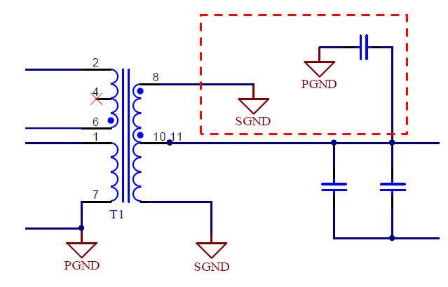
C. Grounding and Return Paths
A solid ground plane helps reduce noise, but high di/dt currents from inductors can induce ground bounce if not managed properly.
✅ Best Practice:
- Use a dedicated ground plane for power components.
- Avoid splitting ground planes beneath inductors to prevent loop inductance.
3. Minimizing EMI and Crosstalk
Switching inductors generate high-frequency noise, which can couple into nearby circuits.
A. Shielding and Spacing
- Use shielded inductors in noise-sensitive designs.
- Maintain sufficient clearance between inductors and sensitive traces (e.g., analog signals, clock lines).
B. Routing Techniques
- Route high-current paths away from control signals.
- Use guard traces or ground shielding for critical signals near inductors.
C. Filtering and Decoupling
- Place input/output capacitors close to the inductor to reduce high-frequency noise.
- Use ferrite beads or additional LC filters if EMI is a concern.
4. Thermal Management and Layout Optimization
Inductors dissipate heat due to core and copper losses, especially in high-current applications.
A. Heat Dissipation Strategies
- Place inductors in areas with good airflow.
- Use thermal vias or heatsinks for high-power designs.
B. PCB Stackup Considerations
- Avoid placing inductors over sensitive inner-layer traces.
- Use thicker copper layers for high-current paths to reduce resistive losses.
5. Common Mistakes and How to Avoid Them
| Mistake | Consequence | Solution |
|---|---|---|
| Long traces between inductor and switch node | Increased EMI and power loss | Minimize loop area |
| Parallel inductor placement | Magnetic coupling and noise interference | Orient inductors perpendicularly |
| Poor grounding | Ground loops and noise injection | Use a solid ground plane |
| Ignoring thermal dissipation | Overheating and reliability issues | Improve airflow and use thermal vias |
Conclusion
Proper inductor placement in power supply PCBs is essential for efficiency, thermal performance, and EMI control. By following these guidelines—minimizing loop areas, optimizing orientation, ensuring proper grounding, and managing heat—designers can achieve robust and high-performance power circuits.
For high-frequency or high-power applications, simulation and prototyping are recommended to validate inductor placement before finalizing the PCB layout


