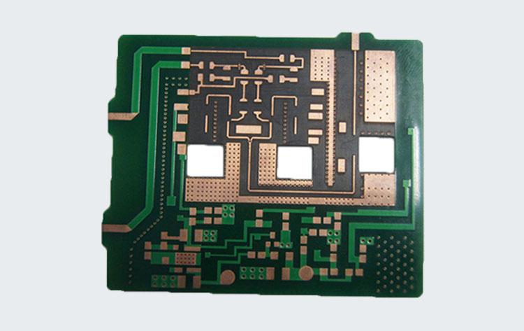
Sample pcb fabrication drawing
Understanding The Basics Of PCB Fabrication Drawings
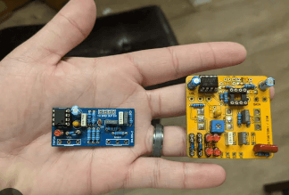
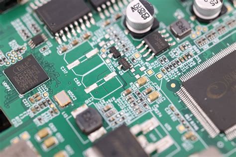
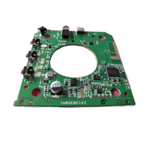
Printed Circuit Board (PCB) fabrication drawings are essential documents in the electronics manufacturing process, serving as a blueprint for the production of PCBs. These drawings provide detailed instructions and specifications necessary for fabricating a PCB, ensuring that the final product meets the design requirements and functions as intended. Understanding the basics of PCB fabrication drawings is crucial for engineers, designers, and manufacturers alike, as these documents bridge the gap between design and production.
To begin with, PCB fabrication drawings typically include a variety of information that guides the manufacturing process.
This information often encompasses the board’s dimensions, layer stack-up, material specifications, and any special instructions that may be pertinent to the fabrication process. By providing a comprehensive overview of the board’s design, these drawings help manufacturers understand the designer’s intent and ensure that the PCB is produced accurately.
One of the key components of a PCB fabrication drawing is the layer stack-up.
This section outlines the arrangement of the various layers within the PCB, including the copper layers, dielectric materials, and any additional layers such as solder mask or silkscreen. The stack-up is crucial because it affects the electrical performance of the PCB, including impedance and signal integrity. By clearly specifying the layer stack-up, designers can ensure that the PCB will function as intended in its final application.
In addition to the layer stack-up, PCB fabrication drawings also detail the board’s dimensions and tolerances.
These specifications are vital for ensuring that the PCB fits correctly within its intended enclosure and interfaces properly with other components. Dimensions are typically provided in both metric and imperial units, allowing manufacturers to work with the measurements that best suit their equipment and processes. Tolerances, on the other hand, indicate the allowable variations in dimensions, ensuring that minor deviations during manufacturing do not affect the board’s functionality.
Material specifications are another critical aspect of PCB fabrication drawings.
These specifications outline the types of materials to be used in the board’s construction, including the substrate, copper weight, and any surface finishes. Material selection can significantly impact the performance, durability, and cost of the PCB, making it essential for designers to carefully consider these factors when creating the fabrication drawing. By clearly specifying the required materials, designers can help manufacturers source the appropriate components and ensure that the final product meets the desired quality standards.
Furthermore, PCB fabrication drawings often include special instructions or notes that provide additional guidance to manufacturers.
These instructions may cover a wide range of topics, such as specific manufacturing processes, testing requirements, or handling procedures. By including these notes, designers can address any unique aspects of the PCB that may not be covered by standard manufacturing practices, helping to prevent errors and ensure a smooth production process.
In conclusion, PCB fabrication drawings are a vital component of the electronics manufacturing process, providing the detailed information necessary to produce a functional and reliable PCB. By understanding the basics of these drawings, engineers, designers, and manufacturers can work together more effectively, ensuring that the final product meets the desired specifications and performs as intended. As technology continues to advance and PCBs become increasingly complex, the importance of clear and accurate fabrication drawings will only continue to grow, making it essential for all stakeholders to have a solid grasp of these critical documents.
Key Elements To Include In A Sample PCB Fabrication Drawing
In the realm of electronics manufacturing, a sample PCB (Printed Circuit Board) fabrication drawing serves as a critical document that bridges the gap between design and production. It provides manufacturers with the necessary details to accurately produce a PCB that meets the designer’s specifications. To ensure a seamless transition from design to fabrication, it is essential to include several key elements in a sample PCB fabrication drawing. These elements not only facilitate clear communication but also help in minimizing errors during the manufacturing process.
First and foremost, the fabrication drawing should include a detailed outline of the PCB.
This outline defines the physical dimensions of the board, including its length, width, and thickness. It is crucial to specify the board’s shape, whether it is rectangular, circular, or any other custom shape, as this will guide the cutting and shaping processes. Additionally, the drawing should indicate any cutouts or slots that are required, as these features can significantly impact the board’s functionality and fit within an enclosure.
Another vital component of the fabrication drawing is the layer stack-up information.
This section provides a cross-sectional view of the PCB, detailing the number of layers, the materials used, and the thickness of each layer. By including this information, designers ensure that manufacturers understand the board’s construction, which is essential for achieving the desired electrical performance and mechanical strength. Furthermore, specifying the type of materials, such as FR-4 or Rogers, helps in selecting the appropriate substrates that meet the design’s thermal and electrical requirements.
In addition to the physical and structural details, the fabrication drawing must also include a comprehensive drill drawing.
This part of the document specifies the size, location, and type of all holes on the PCB, including vias, mounting holes, and component lead holes. By providing precise drill information, designers enable manufacturers to accurately create the necessary holes, which are crucial for component placement and electrical connectivity. It is also important to indicate any special plating requirements for these holes, such as through-hole plating or non-plated holes, to ensure proper electrical isolation or conductivity.
Moreover, the drawing should incorporate a detailed solder mask and silkscreen layer information.
The solder mask layer defines the areas of the PCB that need to be covered with a protective coating, preventing solder bridges and short circuits during assembly. The silkscreen layer, on the other hand, provides visual indicators such as component outlines, reference designators, and logos. Including these details in the fabrication drawing aids in the accurate assembly and inspection of the PCB, ensuring that components are placed correctly and that the board is easily identifiable.
Lastly, it is imperative to include a notes section in the fabrication drawing.
This section can convey additional instructions or clarifications that are not easily represented in the graphical elements of the drawing. For instance, notes can specify the required surface finish, such as HASL or ENIG, or highlight any special handling instructions. By providing these supplementary details, designers can address potential ambiguities and ensure that manufacturers have a comprehensive understanding of the project requirements.
In conclusion, a well-prepared sample PCB fabrication drawing is an indispensable tool in the electronics manufacturing process. By including key elements such as the board outline, layer stack-up, drill drawing, solder mask and silkscreen information, and a detailed notes section, designers can facilitate clear communication with manufacturers. This not only helps in minimizing errors but also ensures that the final product meets the intended design specifications, ultimately leading to a successful and efficient production process.
Common Mistakes To Avoid In PCB Fabrication Drawings
In the realm of electronics manufacturing, the precision and clarity of printed circuit board (PCB) fabrication drawings are paramount. These drawings serve as the blueprint for the entire manufacturing process, guiding engineers and technicians in the creation of functional and reliable electronic devices. However, despite their importance, several common mistakes can occur during the preparation of PCB fabrication drawings, potentially leading to costly errors and production delays. By understanding and avoiding these pitfalls, manufacturers can ensure a smoother fabrication process and a higher quality end product.
One prevalent mistake in PCB fabrication drawings is the omission of critical dimensions and tolerances.
Accurate dimensions are essential for ensuring that components fit correctly on the board and that the board itself fits within its intended enclosure. Without precise measurements, manufacturers may face issues with component placement, leading to potential electrical failures or mechanical interference. To avoid this, it is crucial to include all necessary dimensions and specify tolerances that account for manufacturing variations, ensuring that the final product meets design specifications.
Another common error is the lack of clear and comprehensive notes.
Fabrication drawings should include detailed notes that provide additional instructions or clarifications for the manufacturing process. These notes might cover aspects such as material specifications, surface finish requirements, or special handling instructions. Without these details, manufacturers may make incorrect assumptions, resulting in boards that do not meet the intended design criteria. Therefore, it is essential to provide thorough and unambiguous notes to guide the fabrication process effectively.
In addition to dimensions and notes, the proper use of symbols and annotations is critical in PCB fabrication drawings.
Misinterpretation of symbols can lead to significant errors during manufacturing. For instance, incorrect or inconsistent use of layer designations can cause confusion about which layers should be drilled or plated. To prevent such issues, it is important to adhere to industry-standard symbols and conventions, ensuring that all annotations are clear and consistent throughout the drawing.
Furthermore, overlooking the importance of a comprehensive bill of materials (BOM) can lead to significant challenges in the fabrication process.
The BOM should list all components, materials, and parts required for the PCB, along with their specifications and quantities. An incomplete or inaccurate BOM can result in delays as manufacturers scramble to source missing components or rectify incorrect orders. By providing a detailed and accurate BOM, manufacturers can streamline the procurement process and avoid unnecessary disruptions.
Another area where mistakes often occur is in the specification of drill sizes and locations.
Incorrect drill sizes can lead to issues with component mounting, while inaccurate drill locations can cause misalignment and connectivity problems. To mitigate these risks, it is essential to double-check all drill specifications and ensure they align with the design requirements. Additionally, using automated design tools can help verify drill data and reduce the likelihood of human error.
Finally, failing to review and verify the entire fabrication drawing before submission can result in overlooked errors that propagate through the manufacturing process.
A thorough review process, involving multiple stakeholders, can help identify and correct mistakes before they impact production. By implementing a robust review protocol, manufacturers can enhance the accuracy and reliability of their PCB fabrication drawings.
In conclusion, avoiding common mistakes in PCB fabrication drawings is crucial for ensuring a successful manufacturing process. By paying careful attention to dimensions, notes, symbols, the BOM, drill specifications, and conducting thorough reviews, manufacturers can minimize errors and produce high-quality PCBs that meet design expectations.
How To Optimize Your PCB Fabrication Drawing For Manufacturing Efficiency
Optimizing your PCB fabrication drawing for manufacturing efficiency is a crucial step in ensuring that your printed circuit board (PCB) is produced accurately, cost-effectively, and within the desired timeframe. A well-prepared fabrication drawing serves as a comprehensive guide for manufacturers, providing all the necessary details to produce the PCB without ambiguity or error. To achieve this, it is essential to focus on clarity, completeness, and standardization in your documentation.
To begin with, clarity in your PCB fabrication drawing is paramount.
This involves using clear and precise language, as well as standardized symbols and notations that are universally understood in the industry. By doing so, you minimize the risk of misinterpretation, which can lead to costly errors and delays. It is advisable to use a consistent format throughout the drawing, ensuring that all dimensions, tolerances, and specifications are easily readable. Additionally, including a legend or key for any symbols or abbreviations used can further enhance understanding.
Moreover, completeness is another critical aspect of an optimized PCB fabrication drawing.
This means providing all the necessary information that a manufacturer would need to produce the PCB accurately. This includes, but is not limited to, the board outline, layer stack-up, material specifications, drill sizes and locations, solder mask and silkscreen details, and any special instructions or requirements. By ensuring that your drawing is comprehensive, you reduce the likelihood of back-and-forth communication with the manufacturer, which can save both time and resources.
In addition to clarity and completeness, standardization plays a vital role in optimizing your PCB fabrication drawing.
Adhering to industry standards, such as those set by the Institute for Printed Circuits (IPC), can greatly enhance the manufacturability of your PCB. These standards provide guidelines on various aspects of PCB design and fabrication, ensuring that your drawing aligns with industry best practices. By following these standards, you not only facilitate smoother communication with manufacturers but also increase the likelihood of achieving a high-quality end product.
Furthermore, incorporating design for manufacturability (DFM) principles into your PCB fabrication drawing can significantly enhance manufacturing efficiency.
DFM involves designing your PCB in a way that simplifies the manufacturing process, reduces costs, and improves yield. This can include optimizing the layout for efficient assembly, selecting materials that are readily available and cost-effective, and designing for ease of testing and inspection. By considering these factors during the design phase, you can create a fabrication drawing that supports efficient production.
Transitioning from design to production, it is also beneficial to engage in open communication with your manufacturer.
Sharing your fabrication drawing with them early in the process allows for valuable feedback and potential adjustments that can further optimize manufacturability. Manufacturers can provide insights into their specific capabilities and limitations, which can inform any necessary modifications to your design or drawing.
In conclusion, optimizing your PCB fabrication drawing for manufacturing efficiency involves a careful balance of clarity, completeness, standardization, and design for manufacturability principles. By focusing on these elements, you can create a drawing that not only guides the manufacturer accurately but also contributes to a streamlined production process. This approach not only saves time and resources but also enhances the overall quality and reliability of the final product.