Flow chart of pcb manufacturing process
Understanding The Basics: A Beginner’s Guide To PCB Manufacturing Flow Charts
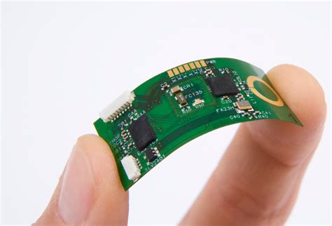
Printed Circuit Boards (PCBs) are the backbone of modern electronic devices, serving as the foundation upon which electronic components are mounted and interconnected.
Understanding the flow chart of PCB manufacturing is crucial for anyone interested in electronics, as it provides insight into the intricate processes that transform raw materials into functional circuit boards.
The journey begins with the design phase, where engineers use specialized software to create a schematic diagram and layout of the PCB.
This design is then translated into a format suitable for manufacturing, typically a Gerber file, which contains all the necessary information about the board’s layers, traces, and component placements.
Once the design is finalized, the manufacturing process commences with the selection of the base material, usually a fiberglass-reinforced epoxy laminate known as FR-4. This substrate provides the structural support for the PCB. The next step involves the application of a thin layer of copper to both sides of the substrate, which will form the conductive pathways. This is achieved through a process called lamination, where heat and pressure are applied to bond the copper to the substrate.
Following lamination, the PCB undergoes a process known as photoresist application.
A light-sensitive film is applied to the copper surface, and the board is exposed to ultraviolet light through a photomask that represents the desired circuit pattern. The exposed areas of the photoresist harden, while the unexposed areas remain soft and are subsequently removed, revealing the underlying copper. This step is crucial as it defines the circuit pattern that will be etched onto the board.
Etching is the next phase, where the exposed copper is removed using a chemical solution, leaving behind only the desired circuit traces protected by the hardened photoresist.
After etching, the remaining photoresist is stripped away, revealing the copper traces that form the electrical pathways of the PCB. To ensure electrical connectivity between different layers of the board, holes are drilled at specific locations, and these holes are plated with copper to create vias.
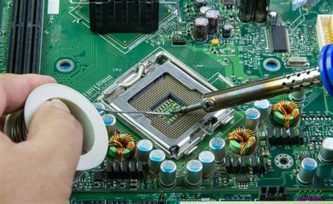
The PCB then undergoes a solder mask application, where a protective layer is applied to insulate the copper traces and prevent solder bridges during component assembly. This is followed by the application of a silkscreen layer, which adds labels and markings to the board, aiding in component placement and identification. At this stage, the PCB is almost complete, but it must undergo a series of inspections and tests to ensure quality and functionality.
Electrical testing is conducted to verify that the circuit paths are correctly formed and that there are no short circuits or open connections.
This is a critical step, as any defects could lead to malfunctioning devices. Once the PCB passes these tests, it is ready for the final stage: surface finish application. This involves coating the exposed copper areas with a protective layer, such as gold or silver, to enhance solderability and prevent oxidation.
In conclusion, the flow chart of PCB manufacturing outlines a complex series of steps that transform a conceptual design into a tangible product. Each phase is meticulously executed to ensure the reliability and performance of the final circuit board. Understanding this process not only demystifies the creation of PCBs but also highlights the precision and expertise required in modern electronics manufacturing.
Key Steps In The PCB Manufacturing Process Flow Chart
The printed circuit board (PCB) manufacturing process is a complex and intricate procedure that involves several key steps, each crucial to the creation of a functional and reliable PCB. Understanding the flow chart of this process is essential for anyone involved in electronics design and production.
The journey begins with the design phase, where engineers use specialized software to create a detailed schematic of the circuit. This schematic is then translated into a layout that specifies the placement of components and the routing of electrical connections on the board.
Once the design is finalized, the next step is to prepare the materials.
This involves selecting the appropriate substrate, typically a fiberglass-reinforced epoxy laminate, which serves as the base of the PCB. The substrate is then coated with a thin layer of copper on both sides, which will form the conductive pathways. Following this, the board undergoes a cleaning process to remove any contaminants that could affect the adhesion of subsequent layers.
The subsequent step in the PCB manufacturing process is the application of a photosensitive resist.
This is achieved by laminating a photosensitive film onto the copper-clad board. The board is then exposed to ultraviolet light through a photomask that represents the desired circuit pattern. The areas exposed to light harden, while the unexposed areas remain soft and are subsequently removed during the development process, revealing the copper beneath.
Etching is the next critical phase, where the exposed copper is removed using a chemical solution, leaving behind only the copper traces that form the circuit.
This step is followed by the stripping of the remaining photoresist, ensuring that only the desired copper pattern remains on the board. At this point, the board undergoes a thorough inspection to ensure that the etching process has been executed correctly and that there are no defects in the circuit pattern.
Drilling is the next step in the process, where holes are created for component leads and vias, which are used to connect different layers of the PCB.
Precision drilling machines are employed to ensure accuracy and consistency in hole placement. Once drilling is complete, the board is plated with a thin layer of copper to ensure electrical connectivity between layers.
The process continues with the application of a solder mask, which is a protective layer that prevents solder from bridging between conductive traces and causing short circuits. The solder mask is applied over the entire board, except for the areas where components will be soldered. This is followed by the application of a silkscreen layer, which provides labels and markings to assist in component placement and identification.
Finally, the PCB undergoes a series of electrical tests to verify its functionality and ensure that there are no short circuits or open connections.
Once testing is complete, the board is ready for assembly, where components are soldered onto the board to create a complete electronic device. Throughout the entire PCB manufacturing process, quality control measures are implemented to ensure that each board meets the required specifications and standards.
In conclusion, the PCB manufacturing process is a meticulous and multi-step procedure that transforms a design concept into a tangible and functional electronic component. Each step in the flow chart is interconnected, with the success of one phase relying on the precision and accuracy of the previous steps. Understanding this process is essential for producing high-quality PCBs that meet the demands of modern electronic applications.
Common Challenges In PCB Manufacturing And How Flow Charts Help
In the intricate world of printed circuit board (PCB) manufacturing, numerous challenges can arise, often complicating the production process and affecting the final product’s quality. These challenges range from design complexities and material selection to precision in fabrication and testing. As the demand for more compact and efficient electronic devices grows, manufacturers face increasing pressure to deliver high-quality PCBs while minimizing errors and production costs. In this context, flow charts emerge as invaluable tools, offering a structured approach to navigating the complexities of PCB manufacturing.
One of the primary challenges in PCB manufacturing is ensuring design accuracy.
The design phase is critical, as any errors can lead to costly revisions and delays. Flow charts help mitigate this risk by providing a clear visual representation of each step in the design process. By outlining the sequence of actions and decision points, flow charts enable designers to systematically verify each aspect of the design, ensuring that all specifications are met before moving on to the next stage. This structured approach not only reduces the likelihood of errors but also facilitates communication among team members, ensuring that everyone is aligned with the project’s objectives.
Another significant challenge is material selection, which can greatly impact the performance and durability of the final product.
With a wide array of materials available, each with its own set of properties and cost implications, making the right choice can be daunting. Flow charts assist in this decision-making process by mapping out the criteria for material selection, such as thermal conductivity, dielectric constant, and mechanical strength. By following a logical progression of considerations, manufacturers can make informed decisions that balance performance requirements with budget constraints.
Precision in fabrication is yet another hurdle in PCB manufacturing.
The intricate nature of PCBs demands exacting standards in etching, drilling, and layering processes. Any deviation can result in defective boards that fail to meet quality standards. Flow charts play a crucial role here by delineating each step of the fabrication process, from initial setup to final inspection. This detailed roadmap ensures that all necessary procedures are followed meticulously, reducing the risk of errors and enhancing overall efficiency. Moreover, flow charts serve as a valuable training tool for new employees, providing them with a clear understanding of the manufacturing process and the importance of adhering to established protocols.
Testing and quality assurance are also critical components of PCB manufacturing, as they ensure that the final product meets all required specifications and functions as intended.
Flow charts streamline this phase by outlining the various testing procedures and criteria for evaluation. By following a structured testing protocol, manufacturers can systematically identify and address any defects or inconsistencies, thereby improving the reliability and performance of the PCBs.
In conclusion, while PCB manufacturing presents a host of challenges, flow charts offer a practical solution by providing a clear and organized framework for managing the complexities of the process. By enhancing design accuracy, guiding material selection, ensuring precision in fabrication, and streamlining testing procedures, flow charts help manufacturers overcome common obstacles and achieve their production goals. As the industry continues to evolve, the use of flow charts will remain a vital component in the quest for efficiency and excellence in PCB manufacturing.
Optimizing Efficiency: Streamlining PCB Production With Flow Charts
In the realm of electronics manufacturing, the production of printed circuit boards (PCBs) is a critical process that demands precision and efficiency. As the backbone of electronic devices, PCBs require meticulous attention to detail during their manufacturing to ensure functionality and reliability.
One effective method to enhance the efficiency of PCB production is through the use of flow charts.
These visual tools serve as a roadmap, guiding manufacturers through each step of the process while highlighting areas for potential improvement.
Flow charts offer a clear and concise representation of the PCB manufacturing process, breaking it down into distinct stages.
This visualization aids in identifying bottlenecks and redundancies, thereby facilitating a more streamlined operation. By mapping out the entire process, from design to final inspection, manufacturers can pinpoint specific areas where time and resources may be optimized. This not only enhances productivity but also reduces the likelihood of errors, which can be costly and time-consuming to rectify.
The initial stage in the PCB manufacturing process involves the design and layout of the circuit board.
Here, engineers utilize computer-aided design (CAD) software to create a detailed blueprint of the PCB. Flow charts can be particularly beneficial at this stage by ensuring that all design specifications are met and that the layout is optimized for manufacturing. Transitioning from design to production, the next step involves the preparation of the raw materials, such as copper-clad laminates, which form the substrate of the PCB.
Subsequently, the process moves to the etching stage, where unwanted copper is removed to reveal the desired circuit pattern.
Flow charts can help streamline this stage by outlining the precise sequence of chemical treatments and rinses required to achieve optimal results. Following etching, the drilled holes for component leads and vias are created, a step that demands high precision. Here, flow charts can assist in coordinating the drilling process, ensuring that it aligns seamlessly with the design specifications.
As the manufacturing process progresses, the next critical phase is the application of solder mask and silkscreen.
The solder mask protects the copper traces from oxidation and prevents solder bridges during component assembly. Flow charts can guide the application process, ensuring uniform coverage and adherence to quality standards. The silkscreen, which provides component labels and other markings, is applied next, and flow charts can help maintain consistency and accuracy in this stage.
The penultimate stage involves the assembly of components onto the PCB.
This step is crucial, as it directly impacts the functionality of the final product. Flow charts can be instrumental in organizing the assembly process, detailing the sequence in which components are placed and soldered onto the board. This ensures that the assembly is conducted efficiently and that any potential issues are addressed promptly.
Finally, the PCB undergoes rigorous testing and inspection to verify its performance and quality.
Flow charts can aid in this stage by outlining the specific tests required and the criteria for passing each test. By providing a structured approach to testing, flow charts help ensure that only PCBs meeting the highest standards are approved for distribution.
In conclusion, flow charts are invaluable tools in optimizing the efficiency of PCB manufacturing. By offering a clear and structured overview of the entire process, they enable manufacturers to identify and address inefficiencies, reduce errors, and enhance overall productivity. As the demand for high-quality electronic devices continues to grow, the role of flow charts in streamlining PCB production becomes increasingly significant, underscoring their importance in the modern manufacturing landscape.