PCB Design for EMC: Layout Techniques to Pass Radiated Emissions Testing
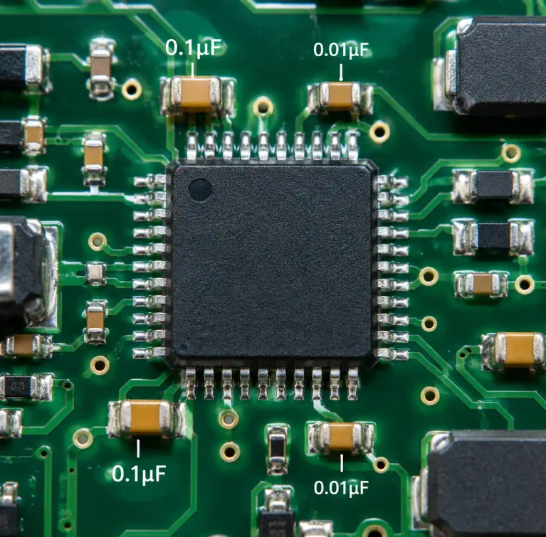
Radiated emissions failures account for roughly 60% of all first-time EMC test failures in my experience working with over 200…

Radiated emissions failures account for roughly 60% of all first-time EMC test failures in my experience working with over 200…
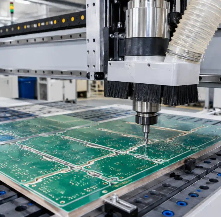
When manufacturing PCBs at scale, multiple boards are fabricated on a single panel to maximize efficiency. The critical question then…
Flux residue accounts for 75% of post-assembly contamination issues leading to field failures in consumer electronics. During reflow and wave…
Every fabrication line relies on tooling holes to register panels across drilling, imaging, and lamination. A 0.1mm registration error on…
Electrostatic discharge (ESD) remains one of the most persistent and costly failure mechanisms in modern electronics. Despite decades of industry…
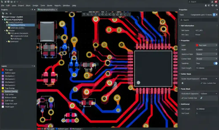
PCB teardrops are teardrop-shaped copper fills added at the junction between traces and pads or vias. Industry data shows that…
Layer count decisions impact 60% of PCB manufacturing costs and directly determine routing success for high-density designs. Engineers face a…
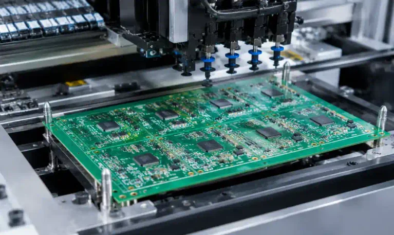
Pick-and-place machines placing 30,000 components per hour achieve 25-micron accuracy only when vision systems lock onto precise reference points. PCB…
Manufacturing a PCB without proper Design for Manufacturing (DFM) review is like sending Gerber files into a black box—you’ll only…
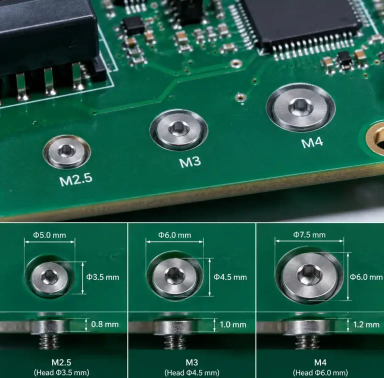
When your PCB assembly requires flush-mounted hardware, choosing between countersink and counterbore holes directly impacts mechanical strength, manufacturing cost, and…
Warped PCBs lead to assembly failures, component misalignment, and rejected production runs. A 2025 industry survey found that copper imbalance…
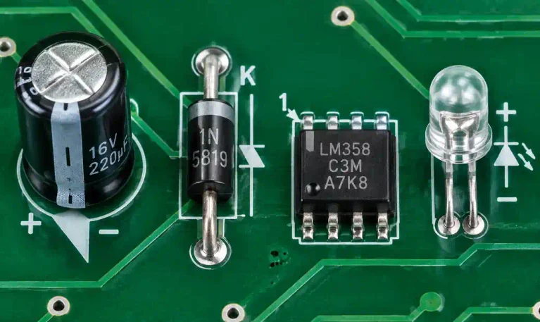
Assembly technicians lose an average of 15-30 seconds per component when silkscreen markings are unclear or missing. On a 200-component…
When designing modular PCB systems or RF shielding enclosures, how do you create reliable electrical connections along the board edge?…
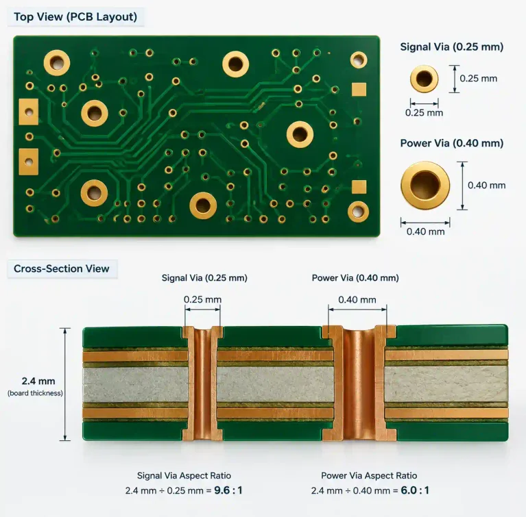
Manufacturing defects in through-hole plating account for 15-20% of PCB failures in multilayer boards. The root cause often traces back…
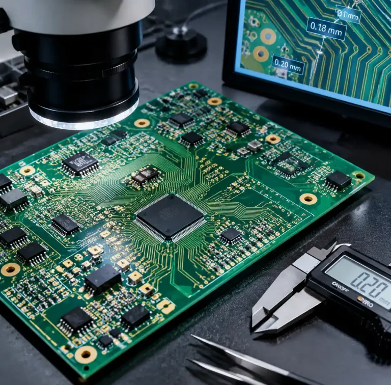
A 3mil/3mil trace-and-space design on Class 3 medical devices costs 45-60% more than 5mil/5mil equivalents, yet most hardware teams default…